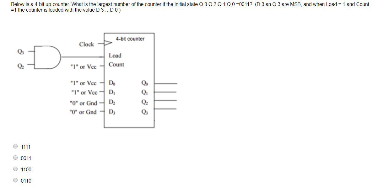
Below is a 4-bit up-counter. What is the largest number of the counter if the initial state Q 3 Q 2 Q1Q0 =0011? (D 3 an Q 3 are MSB, and when Load = 1 and Count =1 the counter is loaded with the value D 3 ...D0) 4-bit counter Clock Q3 Load Count "I" or Vcc "I" or Vcc Do "1" or Vcc - D, Qi Q2 "0" or Gnd - D2 "0" or Gnd D3 Q3 1111 0011 1100 0110


Q: he input to a combinational logic circuit is 4-bit binary number (A, B, C, D). Design the circuit…
A: K map for output Y1 is given as, output Y1 = A
Q: Determine which of the logic circuits in Figure bellow are equivalent. O O Select one: O O O C D' B'…
A: Given logic circuit:
Q: if332to base10=x to base8 then find the value of X.(c)1001011.0112 to equivalent decimal
A:
Q: The D latch of Figure 1 is constructed with four NAND gates and an inverter. Consider the following…
A: It is given that:
Q: Q4/ design logic counter up-down of (1, 2, 5, 8, 9, 10, 12, 14, and 15)
A: Here it is asked to design an up counter where the counting states are given. Here asynchronous…
Q: (a) Figure Q4(a)(i) shows two unit of 74LS293 (4-bit binary counter) configured to generate multiple…
A:
Q: 4. A 4-input MUX is shown on the left below. The logic gate diagram is shown below it, FYI. For the…
A: For the given multiplexer circuit we have to complete the timing diagram
Q: 5.1 Draw the logic diagram for a D FF using only NOR gates. 5.2 The waveform shown below is…
A: 5.1 D ff using NOR gates
Q: Show your solutions clearly and systematically. The D latch of Figure 1 is constructed with four…
A: Given, The D-latch using NAND gate only is shown below,
Q: Show your solutions clearly and systematically. The D latch of Figure 1 is constructed with four…
A: The given D-latch circuit using NAND gate is shown below,
Q: The number $5678 resides in data RAM $300 and $301 in little endian order. The number $1234 resides…
A: CODE IN AVR:
Q: Suppose the waveforms iare those of an ECL gate with VL = −2.6 V andVH = −0.6 V, and t1 = 100 ns, t2…
A: The ∆V is the difference between VH and VL: Thus, the value of V90% and V10% are respectively:
Q: A 9 bit asynchronous counter has a 128 - kHz clock signal applied. i) What the mod Number of this…
A: i) The given asynchronous counter is 9 bits. The mod number of the counter is given as: Mod…
Q: 1:The output of a logic gate is 1 when all the input are at logic 1 and a . OR and EX - NOR Gate b .…
A: Dear student as per our guidelines we are supposed to solve only one question.kindly repost other…
Q: For the circuit shown, a closed switch is represented by a logic 1, and an open switch by a logic 0.…
A: series switches are are named as a AND Gate. Parallel switches are called as OR gate. W and X…
Q: :) A (4-bit) binary counter is connected with DAC to generate a Saw tooth Signal with Frequency of…
A: Given data : Number of bit n=4 Saw tooth signal frequency = 10kHz
Q: a) Write the truth table and logical expression for a two-input AND gate. b) Draw the IC pin diagram…
A: Note: Since you have not specified any question to be answered, as per our honor code, we are…
Q: 1. Convert 95610 to hexadecimal. 2. Convert 1011.101 base 2 to decimal. 3. Convert 110100112 to…
A: Calculate given conversions from decimal to hexadecimal and binary to decimal, decimal to octal and…
Q: Design a 8-to-3 Priority Encoder with the following priority condition D6>D7>D8>D5>D4>D3>D2>D1>D0…
A: Priority Encoder: A priority encoder or digital encoder is also called a Binary encoder that takes…
Q: VpD d) For the given circuit Fill the truth table and identify the type of logic gate Q3 For the…
A: In this question we are asked to fill the table. and then identify the gate. that FET's given are…
Q: Determine the output Q in each of the following logic diagram 9. A=1, B=0, C=1, D=1_ then Q=? 10.…
A:
Q: a) Write the truth table and logical expression for a two-input EX-OR gate. b) Draw the IC pin…
A:
Q: A 9-bit asynchronous counter has a 128-kHz clock signal applied. (i) What is the MOD number of this…
A: Given here a 9-bit asynchronous counter has a 128-kHz clock signal and here we have to find the mod…
Q: What is the step size for a 32 V range, 5 bit digit?
A: Given, Dynamic range (DR) = 32 V Number of bits for each level (n) = 5 Step size=?
Q: (b) Using a synchronous binary counter as shown in Figure Q2(b), design and draw a counter to…
A: The synchronous counter is a electronic circuit which is based on binary logic of signals. This is…
Q: As shown in figure below, that give use the memory circuit of 8086 microprocessor, what is the total…
A:
Q: For the circuits shown in figures 1 and 2:- What is the function of output? 2. Find the max. and…
A:
Q: answere fast please question from DIGITAL LOGIC DESIGN TOPIC : Designing Combinational Logic You…
A: In the design, there is the representation of the water level circuit which indicates the water…
Q: Task 2: praw pinouts of 8088 or 8086 microprocessor (µp). Also draw schematics of 8088/8086 µp buses…
A: to find the 8086 microprocessor architecture
Q: Show your solutions clearly and systematically. The D latch of Figure 1 is constructed with four…
A: Given The D latch of Figure 1 is constructed with four NAND gates and an inverter. Consider the…
Q: a) Using an SR latch and logic gates, design an SN-flipflop which has two input lines (S and N) and…
A: A flip flop is an electronic device having two stable states and it can be used to store binary…
Q: (CLOCK and Data in) to the circuit. AD A1 Function generator A9 A10 A11 A3 A12 AS A13 A6 A14 AT…
A:
Q: If R0 = 0x20008000, after run STMDB r0!, {r3, r9, r7, r1, r2} command what is the r7 register memory…
A: According to the question, we need to find the memory start address for the resister r7.
Q: Address Data ex8007 Ox79 ex8006 OXCD Өx8005 ӨХАЗ RO = 0x8000 and the memory data placement is as…
A: Given: R0=0x8000 and the memory data placement is as follows: To find: What is the order of r1 and…
Q: 1-With most monostable multivibrators, what is the output when no input trigger has 2- The bit…
A:
Q: 1What will be the state of a MOD64 counter after 90 input pulses if the starting state=000000?…
A: As per our company guidelines we are supposed to answer only first question kindly repost other…
Q: Design a combinational circuit that has 4-input (A.B.C.D) and one output (F) the output will be high…
A: STANDARD SUM OF PRODUCT FORM: In standard SOP form, the function is the sum of a number of product…
Q: 1. In the following diagram, you have the architecture of the Intel 8086 questions: Briefly the…
A: Given: In the following diagram, the architecture of the Intel 8086 microprocessor is shown: To…
Q: In a 4-bit ripple up-counter how many clock pulses will you apply, starting from state 0 0 0 0, so…
A:
Q: b) Use the ALU 74181 in the figure below and the tables (one is enough; second maybe, need to check…
A: To analyse the given condition
Q: Use 8086 Microprocessor to execute an instruction MOV [BX}, CX, where (BX] = 0004H, and [DS]=2000H.…
A: Since you have posted a question with multiple subparts, we will solve the first four parts for you.…
Q: on BE RA= 0.7V, V, (sat) 0.8V, Vcz (sat = 0.15V,V SED on) =0.3V, 0 = 0.85, B = 0.25 BC BE Q4. Open…
A: open collector logic gate is shown above and which logic function is performed here
Q: What is the value for the 32-bit register EAX after executing the mnemonic opcode/operand…
A: What is the value for the 32-bit register EAX after executing the mnemonic opcode/operand…
Q: What are the values of the inputs a, b, c, d, e, f and g for a Seven-Segment LED that displays the…
A:
Q: Q4 (a) Figure Q4(a)(i) shows two unit of 74LS293 (4-bit binary counter) configured to generate…
A:
Q: If a 10-bit ring counter has an initial state 1101000000, what is the state after the ?second clock…
A: We need to find out the output state of ring counter
Q: 1. Numbers, Codes, Logic, Circuits a) Convert 101001012 to decimal. b) Convert -6310 to binary using…
A: The solution is given below
Q: Q3. Consider the following 1-bit ALU Operation -Result a. Add additional hardware to this ALU to…
A: The given 1-bit ALU is shown below,
Q: 14.) Using rising edge JK-Flipflops and Digital Logic Gates, build a 4-Stage Shift Register. I…
A: By using rising edge JK-Flip flops and the Digital Logic Gates Building a 4-stage Shift Registor is…


Trending now
This is a popular solution!

Step by step
Solved in 3 steps with 2 images

- Draw pinouts of 8088 or 8086 microprocessor (μp). Also draw schematics of 8088/8086 μp buses with Latch(s) [IC: 74LS373] and Buffer(s) [IC: 74LS245]. Write purpose of using latch and buffer ICs with μp buses. Please Answer all partsHow to build this circuit? (on Digital or Logisim) Binary-coded decimal is an alternative method of representing integers using binary. In it, each base-10 digit is represented by four bits, thus each nibble takes one of 10 values (0000 through 1001). Therefore, using BCD, 42 (decimal) is represented as 0100 0010 (binary) and 196 (decimal) is represented as 0001 1001 0110 (binary). Create a circuit in Logisim that accepts as input a pair of two-digit integers represented as BCD and outputs their sum in BCD. Any and all Digital components are fair game. You can assume that all inputs will be valid BCD-encoded numbers.Behavioural Up Counter With Max Design and implement a 8-bit resetable up count, that stops counting when max is reached. The ports are: module counter( output u8_t count, input u8_t max, input logic clk, reset); The u8_t type is defined in the test bench. count is the counter's output. The counter should increment by one for even positive edge clock until the max is reached. The counter should not increment when max is reached. The counter is reset if reset = 1 when a positive edge clock occurs. The 8-bit comparator module, cmp, must be used to check when max is reached. The test bench will set max to 150 for its testing. Editor // include cmp module module counter( output u8_t count, input u8_t max,input logic clk, reset);logic m_test; cmp test(m_test, count, max); // complete the restendmodule
- Design a 4-bit arithmetic circuit, with two selection variables S1 and S0, that generates the arithmetic operations in the following table. Draw the logic diagram for a single bit stage. Note that B’ represents “Not B”. Draw the logic diagram for a single bit stagWe want to convert a 4 bit ripple counter to a MOD 9 counter. This can be done by? a. Resetting the counter when it reaches 8 b. Resetting the counter when it reaches 9 c. Resetting the counter when it reaches 10 d. A 4-bit counter cannot be turned into a MOD 9 counterso we were asked to implement a 3-bit BCD number on DE0’s board segment display for quartus... using 7447 but 7447 has 4 inputs? (see attached screenshot for problem) also not sure what the items in the second screenshot should be doing? like i can put inputs and outputs..but i don't know what they are? and its not discussed other than they can supply power?
- 1:The output of a logic gate is 1 when all the input are at logic 1 and a . OR and EX - NOR Gate b . AND Gate and EX - OR Gate C. OR and EX - OR Gate d . NAND and OR Gate 2: Choose an application of A / D convertor a. Sonar systems b. Radars and Jammers C. Digital Audio apllications d. Encoders 3: Find the simplification of AB + B ( B + C ) + C ( B + C ) a. C + A b. B + C c. 1 d. A + 4: Choose a correct number of input lines for a decoder which has 128 output lines a . 14 b . 7 c . 1 d . 128 6: Select a suitable example for sequential logic circuit . a . Encoder b . None of the given choices c . Counters d . PALConvert the binary number (1011101) to its equivalent decimal and BCD values. (Show you work) Convert the decimal number (478) to its equivalent hexadecimal and binary values. (Show you work) List the next twenty five hex numbers in sequence from (9E7) hex upwards, adding one each time. (Write them horizontally, with comma as separator) Answer the following logic operations : a) 0 . Z’ = b) 1 + W = c) d . d’ = d) b . b = e) X + (X+1)’ = f) 1 + X’ = g) C + B’C’ = h) B + (BC)’ =…DIGITAL LOGICGiven the two binary numbers X = 1000100 and Y = 100101 , perform the subtraction X - Y by using 1's complement and 2's complement.
- Design a binary multiplier that multiplies two 8-bit binary number by following design rules thatshown in class. The Q and B are the two separate 8-bit binary inputs, C is the 3-bit sequence counterand R is the 16-bit result. (Note: Explain the registers that you will use to establish given process.) The steps are writing algorithm Drawing circuit undetailed (Just use the box, which have only writin under that their functions) Draw logic circuits one by one showing the internal structure of the boxes. Mahe flow chards for registersQ1) Design a counter that has clk and rst as input and 4 bit output. The counter counts in the following sequence: 2-5-8-11-14-1-4-7-10-13-0-3-6-9-12-15Defferentiate comparatively the analogue and digital representations.(b)if332to base10=x to base8 then find the value of X.(c)1001011.0112 to equivalent decimal (d)what do you know about the logic gates?explain the AND gate in details.