Consider the below sequential circuit to determine the values of state diagram of the circuit. Note: if needed, save the picture to your PC and zoom to see better Note: in states, A is the most significant and B is the least significant X-0
Consider the below sequential circuit to determine the values of state diagram of the circuit. Note: if needed, save the picture to your PC and zoom to see better Note: in states, A is the most significant and B is the least significant X-0

Chapter4: Processor Technology And Architecture
Section: Chapter Questions
Problem 9VE

Related questions

Question
I need the answer as soon as possible
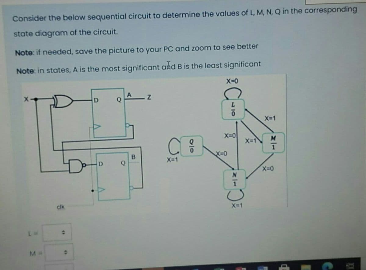
Transcribed Image Text:Consider the below sequential circuit to determine the values of L, M, N, Q in the corresponding
state diagram of the circuit.
Note: if needed, save the picture to your PC and zoom to see better
Note: in states, A is the most significant and B is the least significant
Q
X-1
X-0
X-1
X-D0
Q
X-1
cik
X-1
30
B.
Expert Solution
This question has been solved!
Explore an expertly crafted, step-by-step solution for a thorough understanding of key concepts.

Step by step
Solved in 2 steps

Knowledge Booster


Learn more about
Need a deep-dive on the concept behind this application? Look no further. Learn more about this topic, computer-science and related others by exploring similar questions and additional content below.Recommended textbooks for you
Systems Architecture
Computer Science
ISBN:
9781305080195
Author:
Stephen D. Burd
Publisher:
Cengage Learning
Systems Architecture
Computer Science
ISBN:
9781305080195
Author:
Stephen D. Burd
Publisher:
Cengage Learning