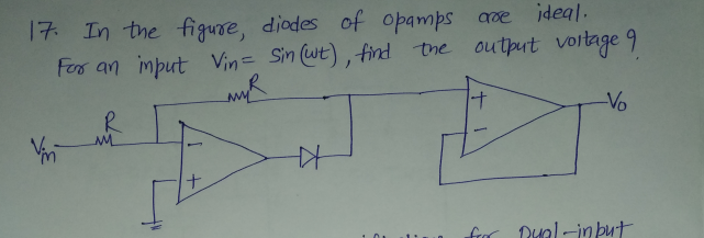
ideal. 17 In the figure, diodes of opamps aoe For an imput Vin= Sin (wt), find voitage 9 the output R. Vo but


Q: (a) Why does a Zener diode work in reverse bias, but a normal diode do not? Explain.
A: In forward biased condition, a Zener diode acts a normal diode in forward biased condition. But in…
Q: (a)
A: In the given circuit diagram, Given value of cutting voltage in forward-bias region is 0.6 V As we…
Q: A 20-V-rms 60-Hz ac source is in series with an ideal diode and a 100-Ω resistance. Determine the…
A: Draw the mentioned circuit diagram.
Q: b) What is the term Break down characteristic in Zener diode with the draw this characteristic?
A: The forward bias characteristics of a zener diode is same as a normal pn junction diode. Where as…
Q: What is zener diode ? With Application of zener diode
A: Zener diodes are semiconductor devices made of silicon that allow current to flow in either…
Q: Sketch the transfer characteristic (vo versus vin) to scale for the circuit shown in FigureP9.66 .…
A: When input voltage is more than 0V, Diode D1 becomes reverse biased and Diode D2 becomes forward…
Q: a) Write down the characteristic equation of a semiconductor diode. b) What happens in a…
A:
Q: Consider the voltage-regulator circuit shown in Figure P9.85. The ac ripple voltage is 1 V peak to…
A: To find the Q-point in the circuit, neglect the ripple voltage and Draw the circuit.
Q: (a) Determine the minimum and maximum input voltages that can maintain the zener diode IN4753A in…
A: To solve above question, one should know about Zener diode and its application. A Zener diode is a…
Q: 2) According to the diode characteristics and load line given in the figure below: a) Find the…
A:
Q: a diode and show these elements on the curve. plain the conditions of cut-off, saturation and linear…
A: Diode- It is the minimum forward voltage across diode after which diode start conduction. Diode is…
Q: Define Drift and Diffusion current in Semiconductor
A: As per guidelines we are supposed to solve only one question (i.e first question). So I request you…
Q: Evaluate output using ideal diode model and constant voltage drop model.
A: In the given questions we need to 1st find the operating conditions of diode.
Q: The diode portion of the following circuit is called a voltage limiter. Explain why. Sketch some…
A: The circuit is as shown below, Given, VH>VL,
Q: Sketch the transfer characteristic (vo versus vin) for the circuit shown in Figure P9.67, carefully…
A: While the diode is reverse biased, let the voltage at node 1 be V1. The equivalent circuit is given…
Q: What happens to an ideal diode when it is reverse biased? In terms of the current flowing through it
A: In this question , we will write about What happens to an ideal diode when it is reverse biased..
Q: An AC voltage peak value of 20 Volts is connected in series with a silicon diode and load resistance…
A: here 20 v source is connected to positive terminal of the battery to make the diode to operate in…
Q: (c ). Design a Diodes Limiting Circuit to limit a 120 Vrms Sinusoidal Voltage Signal to a Maximum…
A: Clipper circuits are voltage limiter circuits that limit the voltage at some particular dc voltage…
Q: As compared to a p-n junction device of equal rating.the schottly diode has? a-higher cut in…
A: For schottky diode
Q: u= 6sinot V. V. For the circuit of Figure, we have known E=3V, Use the ideal diode model to analyze…
A: The diode is ON when the voltage across anode is more than the cathode voltage. It is known as…
Q: Describe in your own words the characteristics of the ideal diode and how they determine the on and…
A: Given: ideal diode explain
Q: Plot the diode reverse characteristic, and estimate an approximate value for the reverse saturation…
A:
Q: Q5- What is the advantage of the Zener diode ?
A:
Q: Find the Q-point for the diodes in Figure QI(a) using the ideal diode model.
A:
Q: 3. Design a clipping circuit that will limit the output voltage to 5V when applying an input…
A: The clipping circuit can be designed by using the diode and the resistors. The diode should be…
Q: Discuss the working principle of a diode and also the equivalent models of a diode.
A:
Q: A sinusoidal voltage of peak value 50 V is applied to a diode as shown in the figure. Sketch the…
A:
Q: What are the V-I characteristics of standard power diode and Schottky Diode ?
A: The V-I characteristics of standard power diode: Forward biased When the diode is forward-biased…
Q: What is a Zener diode? For what is it typically used? Draw the volt–ampere characteristic of an…
A: Given: Zener diode is explained as:
Q: For a silicon pn junction, the reverse saturation current at 20o C is 10 pA. What will be reverse…
A: When the p-n junction diode is operating in the reverse bias mode, then very small amount of current…
Q: Sketch the transfer characteristic vo versus vi for the limiter circuit shown below. All diodes…
A:
Q: Design a clamper circuit that shifts the DC level of an input sinusoidal waveform by +6V if the peak…
A: The Clamper circuit helps to shift the DC Level of input based on our requirements.it contains…
Q: Describe and show full wave rectification using two diodes.
A: Rectifier is a circuit which converts AC voltage into pulsating DC voltage . Full wave Rectifier is…
Q: Explain the importance of the Volt-Ampere Characteristics of P-N Diode
A: Volt-Ampere Characteristics of P-N Diode curve between voltage over junction and circuit current.…
Q: What should be the value of Vi, if we have a Zener Diode with a breakdown voltage of 6.2 volts and a…
A:
Q: Explain AC and DC diode resistance alomg with their formulas and curves.
A: According to the given question, it is required to explain AC and DC diode resistance alomg with…
Q: 6. Design a clamper circuit that shifts the DC level of an input sinusoidal waveform by +6V if The…
A:
Q: What is Shockley-Queisser limit? Explain the upper limit of V oc and short circuit current of single…
A: Solar cells- Solar cells capture energy from the sun and convert it to electricity. The sun is the…
Q: Sketch i versus v to scale for the circuits shown in Figure P9.6. The reverse-breakdown voltages of…
A: Part (a): For the positive voltage, the left diode will be the forward bias, and the right diode…
Q: What is the specialty of Zener diode so as we can operate it in breakdown region for longer…
A: Zener diode is a special purpose diode. This diode is designed to operate in reverse bias and…
Q: Using ideal diodes (voltage drop across ideal diodes is zero) and resistors, construct a circuit…
A:
Q: Discuss the biasing and saturation voltage of a diode. Suggest how one can convert AC to the…
A: Biasing voltage of Diode: Biasing voltage of Diode is defined as the voltage which either allow the…
Q: A 6.3V AC signal is half-wave rectified and applied to a 33-ohm load resistance. Determine the peak…
A:
Q: 1- Explain briefly with figure if exist, the Degenerate semiconductors. 2- When a diode is connected…
A: 1- Semiconductors are those materials that have electrical conductivity in between that of…
Q: Consider the Zener diode circuit shown in Figure. The Zener Breakdown Voltage (Vz) is 5.6 V at Iz=…
A:
Q: Describe the conditions established by forward- and reverse-bias conditions on a p–n junction diode…
A:
Q: 5. Design a clamper circuit that shifls the DC level of an input sinusoidal waveform by +6V if the…
A:
Q: Determine the range of values of Vi that will maintain the Zener diode of Figure.
A: The required parameter of the Zener regulator can be calculated based on the Zener voltage and the…
Q: Q7. What is the specialty of Zener diode so as we can operate it in breakdown region for longer…
A: Since zener diodes are highly doped than a normal diode and hence depletion layer is less wider as…
find the output voltage

Step by step
Solved in 5 steps with 6 images


- Consider the following circuit (See image):Show that it is a unity gain absolute value circuit, consider ideal diodesThe Zener-diode regulator circuit shown below is to be used to provide a stabilised output to the load. The zener diode characteristic is also shown. Find the load voltage and source current if the battery voltage is 24 V, series resistance is 1.2 kohm and load resistance is 6 kohm.As compared to a p-n junction device of equal rating.the schottly diode has? a-higher cut in voltage b-lower reverse leakage current c-lower reverse voltage rating d-higher switching time
- The Zener-diode regulator circuit shown below is to be used to provide a stabilised output to the load. The Zener diode characteristic is also shown. Find the source current if the battery voltage is 24 V, series resistance is 1.8 KΩ and load resistance is 10 KΩ.Npn with a β value of 100 in the circuit in the figurefor zener diodes used to drive the transistorGiven as VZ1=16.7 V and VZ2=5.6 V. Inanalysis of transistor operating point Circuitidentify by.(VBE=0.7 V )Draw a schematic diagram of a forward bias diode.
- Suppose we have a 10-V-peak sinusoidal voltage source. Draw the diagram of a circuit that clips off the part of the sinusoid above 5 V and below -4 V. The circuit should be composed of ideal diodes, dc voltage sources, and other components as needed. Be sure to label the terminals across which the clipped output waveform vo(t) appears.Assume that the diode offset voltage Vγ is 0.4 V and that Rd = 400 Ω. For a loadresistor of 1 k Ω and a sinusoidal input of Vin=2 sin(wt), sketch the output voltage (across theload resistor) over two cycles.Consider the diode circuit shown below. If Vs is a sinewave with a peak amplitude of 12 Volts at 60Hz, and diodes D1 & D2 are considered ideal, sketch the appearance of the waveform at node voltage Vout . Sketch the appearance of the waveform at Vout .
- What is a Zener diode? For what is it typically used? Draw the volt–ampere characteristic of an ideal 5.8-V Zener diode.For the circuit shown below, compute the maximum current through each resistor when terminal A is a) positive and, b) negative. Assume the diodes are ideal. (Will we convert to the RMS value to it's actual value?)The circuit in Figure is a complementary output rectifier. If vs = 26√2sin[120πt]V,assumingV? =0.6V for each diode. Determine the average and rms of complimentary outputs VO+ and VO-. . Also derive formfactor and ripple factor each output.