
Videos
Find I and
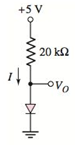
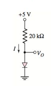
(a).
The values of
Answer to Problem 1.47P
For
For
Explanation of Solution
Given Information:
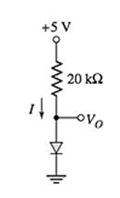
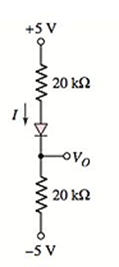
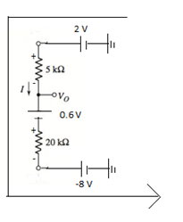
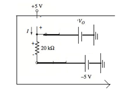
The given circuit is shown below.
Two values of
Calculation:
For
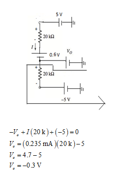
The given circuit diagram is:
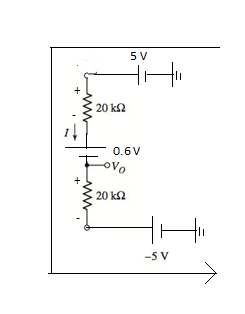
Assuming the diode is in ON state and the modified circuit is:
Applying Kirchhoff’s voltage law:
The direction of current is from p-region to n-region of diode. Hence, the assumption is correct.
Applying Kirchhoff’s voltage law:
For
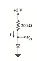
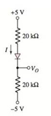
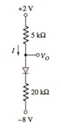
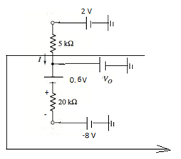
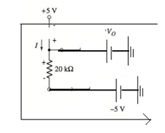
The given circuit diagram is:
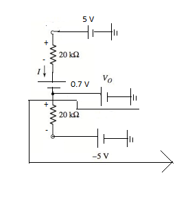
Assuming the diode is in ON state and the modified circuit is:
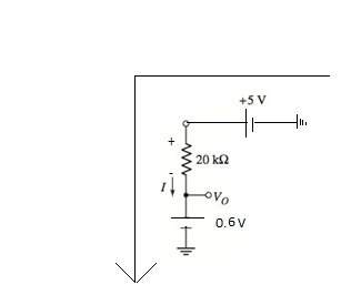
Applying Kirchhoff’s voltage law:
The direction of current is from p-region to n-region of diode. Hence, the assumption is correct.
Applying Kirchhoff’s voltage law:
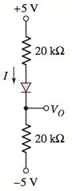
(b).
The values of
Answer to Problem 1.47P
For
For
Explanation of Solution
Given Information:
The given circuit is shown below.
Two values of
Calculation:
For
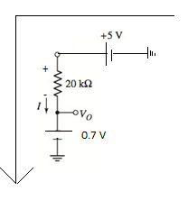
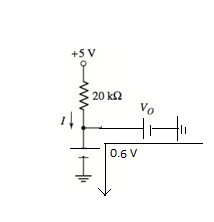
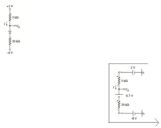
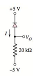
The given circuit diagram is:
Assuming the diode is in ON state and the modified circuit is:
Applying Kirchhoff’s voltage law:
The direction of current is from p-region to n-region of diode. Hence, the assumption is correct.
Applying Kirchhoff’s voltage law in the following circuit:
For
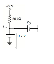
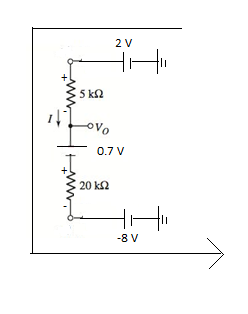
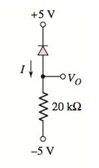
The given circuit diagram is:
Assuming the diode is in ON state and the modified circuit is:
Applying Kirchhoff’s voltage law:
The direction of current is from p-region to n-region of diode. Hence, the assumption is correct.
Applying Kirchhoff’s voltage law in the following circuit:
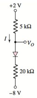
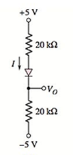
(c)
The values of
Answer to Problem 1.47P
For
For
Explanation of Solution
Given Information:
The given circuit is shown below.
Two values of
Calculation:
For
The given circuit diagram is:
Assuming the diode is in ON state and the modified circuit is :
Applying Kirchhoff’s voltage law:
The direction of current is from p-region to n-region of diode. Hence, the assumption is correct.
Applying Kirchhoff’s voltage law in the following circuit:
For
The given circuit diagram is:
Assuming the diode is in ON state and the modified circuit is:
Applying Kirchhoff’s voltage law:
The direction of current is from p-region to n-region of diode. Hence, the assumption is correct.
Applying Kirchhoff’s voltage law in the following circuit:
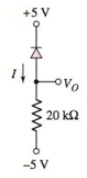
(d).
The values of
Answer to Problem 1.47P
For
For
Explanation of Solution
Given Information:
The given circuit is shown below.
Two values of
Calculation:
For
The given circuit diagram is:
Assuming the diode is in OFF state. Hence, the modified circuit is:

From the circuit:
In this circuit, the diode is reverse biased, so it is in OFF mode. Hence, the assumption is correct and the value of current
Applying Kirchhoff’s voltage law in the following circuit:
For
The given circuit diagram is:
Assuming the diode is in OFF state. Hence, the modified circuit is:
From the circuit:
In this circuit, the diode is reverse biased, so it is in OFF mode. Hence, the assumption is correct and the value of current
Applying Kirchhoff’s voltage law in the following circuit:
Want to see more full solutions like this?
Chapter 1 Solutions
Microelectronics: Circuit Analysis and Design
Additional Engineering Textbook Solutions
Basic Engineering Circuit Analysis
Engineering Electromagnetics
Principles and Applications of Electrical Engineering
Electric Circuits. (11th Edition)
Electronics Fundamentals: Circuits, Devices & Applications
Electric machinery fundamentals


- Using the approximate field calculation in a cylinder-plane electrode system, extract the expression for the maximum electric field strength. Calculate the puncture voltage since the cylinder diameter is 24 mm, the electrode opening is 20 cm, the puncture strength of the air is 30 kV/cm and the correction factor (k) is 0.90arrow_forwardSuppose that NA(x) = No exp(−x/L) in a region of silicon extending from x =0 to x = 8μm,where No is a constant. Assume that p(x) = NA(x). Assuming that jp must be zero in thermale quilibrium, show that a built-in electric field must exist and find its value for L =1 μm and No =1018/cm3.arrow_forwardSolve only a,c & d Use the following constants if necessary. Coulomb constant, k = 8.987×10^9 N⋅m^2/C^2 . Vacuum permitivity, ϵ0= 8.854×10^−12 F/m. Magnetic Permeability of vacuum, μ0 = 12.566370614356×10^−7 H/m. Magnitude of the Charge of one electron, e = −1.60217662×10^−19 C. Mass of one electron, m_e = 9.10938356×10^−31 kg. Unless specified otherwise, each symbol carries their usual meaning. For example, μC means microcoulomb .arrow_forward
- COURSE: HIGH VOLTAGE TECHNIQUE In an insulating environment consisting of insulating oil (Ɛr1=12.5) and porcelain (Ɛr2=2.5), the electric field enters the porcelain environment through the oil at an angle of 50 relative to the normal of the border surface. Since the field strength is 87 kV/cm in oil environment, calculate the electric field strength in the porcelain environment, the tangent and normal components of the electric field strength in both environments. PLEASE MAKE A DETAILED SOLUTION!arrow_forwardCalculate the intrinsic carrier density n, for Silicon at I = 292 K. Show all your work and write your answer with 4 significant figures.arrow_forward20 mm thicknesses and 1500 mm^2 The 200 WATT power of 3 MHz is used to warm up the fragment of the field-made insulating material from dielectric fiting. If this insulating material is the Permitivity 5 and the power factual 0.5, then find the need for this process to pass through the voltage and the mental value.arrow_forward
- The total charge entering a terminal is given by q = 2e3t cos (6\pi t), in µC. Determine the current at t= 0.25 s.arrow_forward2/ for the figure shown below find How much the potential Energy or the work Wa-b which s needed to move the test charge qo from point a to b along the radiallne if :qo= 2nc, 4= 5nc ra= 10 cm, b= 20, And from the value of the work find How much the Potential difference at g7 Testcharge g . moves fromat0b along radial line: fromg. Earrow_forwardWhat are electron,hole,intrinsic carrier concentration, and energy band gap in si with (a) Nd= 4×10¹⁶ cm⁻³ and Na=1×10¹⁶ cm⁻³ and (b) additional 6×10¹⁶ cm⁻³ of ND ? Note: use Effective density of conduction band= 2.8 ×10¹⁹ cm⁻³ .Effective density of valance band =1.04 × 10¹⁹cm⁻³.T=300K ,Boltzmann constant = 1.38 x 10⁻²³ kgs⁻²K⁻¹arrow_forward
- The current entering the upper terminal of a basic circuit element is i=20cos5000t A. Assuming the charge at the upper terminal is zero at the instant the current is passing through its maximum value. What is the expression for the charge q(t)? A)q(t)=16sin5000t mC B)q(t)=16sin10000t mC C)q(t)=16cos5000t mC D)q(t)=4sin5000t mC E)q(t)=20sin5000t mC F)q(t)=20cos5000t mC G)q(t)=40cos10000t mCarrow_forwardLoop Equation I1 Loop I1 Equation: What is the coefficient value associated with the variable, I1? Loop I1 Equation: What is the coefficient value associated with the variable, I2? Loop I1 Equation: What is the constant value for Loop I1 (right side of the equation)? Loop Equation I2 Loop I2 Equation: What is the coefficient value associated with the variable, I1? Loop I2 Equation: What is the coefficient value associated with the variable, I2? Loop What is the calculated Loop I1 value in Amps (tenth-place degree of accuracy)? I2 Equation: What is the constant value for Loop I2 (right side of equation)? What is the calculated Loop I2 value in Amps (tenth-place degree of accuracy)?arrow_forwardExplain the modifciation to be made to the schering bridge for the following situations: i) Hihg dissipation factor test objects II) High capacitance test objects Explain in easy language so i can understandarrow_forward
 Introductory Circuit Analysis (13th Edition)Electrical EngineeringISBN:9780133923605Author:Robert L. BoylestadPublisher:PEARSON
 Delmar's Standard Textbook Of ElectricityElectrical EngineeringISBN:9781337900348Author:Stephen L. HermanPublisher:Cengage Learning
 Programmable Logic ControllersElectrical EngineeringISBN:9780073373843Author:Frank D. PetruzellaPublisher:McGraw-Hill Education
 Fundamentals of Electric CircuitsElectrical EngineeringISBN:9780078028229Author:Charles K Alexander, Matthew SadikuPublisher:McGraw-Hill Education
 Electric Circuits. (11th Edition)Electrical EngineeringISBN:9780134746968Author:James W. Nilsson, Susan RiedelPublisher:PEARSON
 Engineering ElectromagneticsElectrical EngineeringISBN:9780078028151Author:Hayt, William H. (william Hart), Jr, BUCK, John A.Publisher:Mcgraw-hill Education,