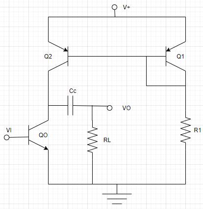
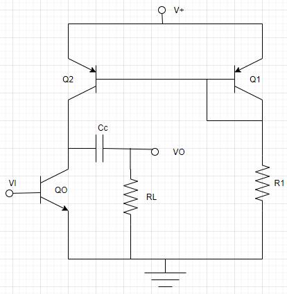
Problem 10.1EP: The circuit parameters for the two-transistor current source shown inFigure 10.2(b) are V+=3V , V=3V... Problem 10.2EP: Consider the circuit shown in Figure 10.3. The circuit parameters are: V+=5V,V=5V , and R1=12k . The... Problem 10.3EP: The parameters of the circuit shown in Figure 10.5 are: V+=3V,V=3V , and R1=30k . The parameters of... Problem 10.4EP: Consider the Widlar current source in Figure 10.9. The bias voltages are V+=3V and V=3V . Design the... Problem 10.5EP: Consider the circuit in Figure 10.10. Assume the reference current is IREF=120A and assume the... Problem 10.6EP: A Widlar current source is shown in Figure 10.9. The parameters are: V+=5V,V=0,IREF=0.70mA ,and... Problem 10.7EP: Figure 10.12 shows the N-output current mirror. Assuming all transistors are matched, with a finite... Problem 10.1TYU Problem 10.2TYU Problem 10.3TYU: For the Wilson current source in Figure 10.8, the transistor parameters are: VBE(on)=0.7V,=50 , and... Problem 10.4TYU Problem 10.8EP Problem 10.9EP Problem 10.10EP: Consider the JFET circuit in Figure 10.24. The transistor parametersare:... Problem 10.5TYU: Consider Design Example 10.8. Assume transistor parameters of... Problem 10.6TYU: The bias voltages of the MOSFET current source in Figure 10.17 are V+=3V and V=3V . The transistor... Problem 10.7TYU Problem 10.8TYU: All transistors in the MOSFET modified Wilson current source in Figure10.20(b) are identical. The... Problem 10.11EP: A simple BJT amplifier with active load is shown in Figure 10.29. Thetransistor parameters are:... Problem 10.9TYU Problem 10.10TYU Problem 10.11TYU Problem 10.12EP Problem 10.13EP: For the circuit in Figure 10.40(a), the transistor parameters are:... Problem 10.12TYU Problem 10.13TYU: Repeat Example 10.12 for the case where a resistor RE=1k is included in the emitters of Q1 and Q2 as... Problem 10.14TYU Problem 1RQ Problem 2RQ: Explain the significance of the output resistance of the current-source circuit. Problem 3RQ Problem 4RQ Problem 5RQ: What is the primary advantage of a BJT cascode current source? Problem 6RQ Problem 7RQ: Can a piecewise linear model of the transistor be used in the analysis of theWidlar current source?... Problem 8RQ Problem 9RQ: Sketch the basic MOSFET two-transistor current source and explain the operation. Problem 10RQ: Discuss the effect of mismatched transistors on the characteristics of theMOSFET two-transistor... Problem 11RQ Problem 12RQ: Sketch a MOSFET cascode current source circuit and discuss the advantages ofthis design. Problem 13RQ: Discuss the operation of an active load. Problem 14RQ: What is the primary advantage of using an active load? Problem 15RQ Problem 16RQ: What is the impedance seen looking into a simple active load? Problem 17RQ: What is the advantage of using a cascode active load? Problem 10.1P Problem 10.2P: The matched transistors Q1 and Q2 in Figure 10.2(a) have parameters IS=1016A . (a) For = , determine... Problem 10.3P Problem 10.4P: Reconsider the circuit in Figure 10.2(a). Let IREF=150A . Assume transistor parameters of... Problem 10.5P Problem 10.6P: The transistor and circuit parameters for the circuit in Figure 10.2(b) are:... Problem 10.7P: The bias voltages in the circuit shown in Figure 10.2(b) are V+=+5V,V=5V and the resistor value is... Problem 10.8P: Consider the current source in Figure 10.2(b). The circuit is biased at V+=2.5V and V=2.5V . The... Problem 10.9P Problem 10.10P Problem D10.11P Problem D10.12P: In the circuit in Figure P10.11, the transistor parameters are =80 and VEB(on)=0.7V . (a) Design the... Problem D10.13P Problem 10.14P: Consider the circuit shown in Figure P 10.14. The transistor Q2 is equivalentto two identical... Problem D10.15P: Design a basic two-transistor current sourcecircuit configuration suchthat IO=0.40mA and IREF=0.20mA... Problem 10.16P: The values of for the transistors in Figure P10.16 are very large. (a) if is diode-connected with... Problem 10.17P: Consider the circuit in Figure P10.17. The transistor parameters are: =80,VBE(on)=0.7V , and VA= .... Problem 10.18P: All transistors in the N output current mirror in Figure P10.18 are matched,with a finite and VA= .... Problem D10.19P: Design a pnp version of the basic three-transistor current source circuit,using a resistor to... Problem D10.20P Problem 10.21P: Consider the Wilson current source in Figure P10.21. The transistors have afinite and an infinite... Problem 10.22P: Consider the circuit in Figure P10.22. The transistor parameters for Q1 and Q2 are VBE1,2(on)=0.7V... Problem 10.23P: Consider the Wilson current-source circuit shown in Figure 10.8. Assumethe reference current is 0.25... Problem 10.24P: Consider the Widlar current source shown in Figure 10.9. The circuit parameters are... Problem 10.25P Problem 10.26P: Consider the circuit in Figure P10.26. Neglect base currents and assume VA= . Assume IREF=100A and... Problem 10.27P: (a) For the Widlar current source shown in Figure 10.9, find IREF,IO , and VBE2 if... Problem 10.28P: Consider the Widlar current source in Problem 10.27. For =80 and VA=80V , determine the change in IO... Problem D10.29P: (a) Design the Widlar current source such that IREF=0.50mA and IO=50A . Assume that V+=+5V , V=5V ,... Problem D10.30P: Design a Widlar current source to provide a bias current of IO=50A .The circuit is to be biased at... Problem D10.31P: Design the Widlar current source shown in Figure 10.9 such that IREF=2mA and IO=50A . Let V+=15V and... Problem 10.32P: The circuit parameters of the Widlar current source in Figure 10.9 are V+=3V,V=3V , and R1=20k .... Problem 10.33P: Consider the Widlar current source in Figure 10.9. The circuit parameters are: V+=10V,V=10V,R1=40k ,... Problem 10.34P: Consider the circuit in Figure P10.34. The transistors are matched. Assumethat base currents are... Problem 10.35P: The modified Widlar current-source circuit shown in Figure P10.34 isbiased at V+=3V and V=3V . (a)... Problem 10.36P: Consider the circuit in Figure P10.36. Neglect base currents and assume VA= . (a) Derive the... Problem 10.37P: Consider the Widlar current-source circuit with multiple output transistors shown in Figure P10.37.... Problem 10.38P: Assume that all transistors in the circuit in Figure P10.38 are matched andthat = (neglect base... Problem 10.39P: In the circuit in Figure P10.39, the transistor parameters are: = , VA= ,and VBE=VEB=0.7V . Let... Problem 10.40P: Consider the circuit in Figure P10.39, with transistor parameters = , VA= , and VBE(on)=VEB(on)=0.7V... Problem 10.41P: Consider the circuit shown in Figure P10.41. Assume VBE=VEB=0.7V for all transistors except Q5 and... Problem 10.42P: For the circuit shown in Figure P 10.42, assume transistor parameters VBE=VEB=0.7V for all... Problem D10.43P: Consider the circuit in Figure P10.43. The transistor parameters are: = , VA= , and VBE=0.7V .... Problem 10.44P: Consider the MOSFET current-source circuit in Figure P10.44 with V+=+2.5V and R=15k . The transistor... Problem D10.45P: The MOSFET current-source circuit in Figure P10.44 is biased at V+=2.0V . The transistor parameters... Problem 10.46P: Consider the basic two-transistor NMOS current source in Figure 10.16.The circuit parameters are... Problem 10.47P Problem 10.48P: Consider the circuit shown in Figure P10.48. Let IREF=200A . The transistor parameters are... Problem 10.49P Problem 10.50P: The circuit parameters for the circuit shown in Figure 10.17 are V+=1.8V and V=1.8V . The transistor... Problem 10.51P Problem 10.52P: Figure P10.52 is a PMOS version of the current-source circuit shown inFigure 10.17. The transistor... Problem D10.53P: The circuit shown in Figure P10.52 is biased at V+=+2V and V=2V . Assume the transistor parameters... Problem 10.54P: The transistor circuit shown in Figure P10.54 is biased at V+=+5V and V=5V . The transistor... Problem D10.55P: Assume the circuit shown in Figure P10.54 is biased at V+=3V and V=3V . The transistor parameters... Problem 10.56P: The circuit in Figure P 10.56 is a PMOS version of a two-transistor MOScurrent mirror. Assume... Problem D10.57P: The transistors in Figure P10.56 have the same parameters as in Problem10.56 except for the W/L... Problem 10.58P: Consider the NMOS cascode current source in Figure 10.18. The circuitparameters are V+=+5V,V=5V ,... Problem 10.59P: Consider the NMOS current source in Figure P10.59. Let IREF=0.2mA , Kn=0.2mA/V2,VTN=1V , and =0.02V1... Problem 10.60P Problem D10.61P: The transistors in the circuit shown in Figure P10.60 have the same parameters as in Problem 10.60... Problem 10.62P: A Wilson current mirror is shown in Figure 10.20(a). The parameters are: V+=+5V , V=5V , and... Problem 10.63P: Repeat Problem 10.62 for the modified Wilson current mirrorFigure 10.20(b). Problem 10.64P Problem 10.65P Problem D10.66P Problem D10.67P Problem 10.68P: The parameters of the transistors in the circuit in Figure P10.68 are... Problem 10.69P Problem 10.70P: Consider the circuit shown in Figure P10.70. The NMOS transistor parameters VTN=0.4V,kn=100A/V2,n=0... Problem 10.71P Problem D10.72P Problem 10.73P Problem D10.74P Problem 10.75P Problem 10.76P: For the circuit shown in Figure P10.76, the transistor parameters are... Problem 10.77P Problem 10.78P Problem D10.79P: The bias voltage of the MOSFET amplifier with active load in FigureP10.79 is changed to V+=3V . The... Problem 10.80P Problem 10.81P Problem 10.82P Problem 10.83P: A BJT amplifier with active load is shown in Figure P10.83. The circuit contains emitter resistors... Problem 10.84P Problem 10.85P Problem 10.86P Problem 10.87P: The parameters of the transistors in Figure P10.87 are VTN=0.6V,VTP=0.6V,kn=100A/V2,kP=60A/V2 , and... Problem 10.88P: The parameters of the transistors in Figure P10.88 are VTN=0.6V,VTP=0.6V,kn=100A/V2,kP=60A/V2 , and... Problem 10.89P: A BJT cascode amplifier with a cascode active load is shown inFigure P10.89. Assume transistor... Problem D10.90P: Design a bipolar cascode amplifier with a cascode active load similar tothat in Figure P10.89 except... Problem D10.91P: Design a MOSFET cascode amplifier with a cascode active load similar tothat shown in Figure P10.88... Problem D10.96DP: Design a generalized Widlar current source (Figure P10.34) to provide abias current of IO=100A and... Problem D10.97DP: The current source to be designed has the general configuration shown inFigure 10.17. The bias... Problem D10.98DP: Designa PMOS version of the current source circuit shown in Figure10.27. The circuit is to be biased... Problem D10.99DP: Consider Exercise TYU 10.10. Redesign the circuit such that the small-signal voltage gain is Av=120... format_list_bulleted


 EBK ELECTRICAL WIRING RESIDENTIALElectrical EngineeringISBN:9781337516549Author:SimmonsPublisher:CENGAGE LEARNING - CONSIGNMENT