
Videos
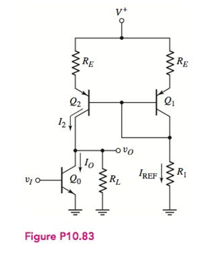
A BJT amplifier with active load is shown in Figure P10.83. The circuit contains emitter resistors
(a)
To derive:An expression for the output resistance
Answer to Problem 10.83P
Explanation of Solution
Given:
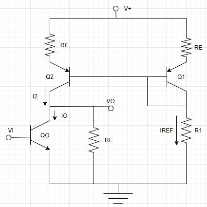
The given circuit is,

Calculation:
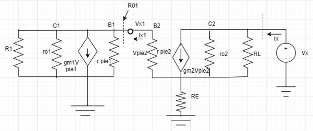
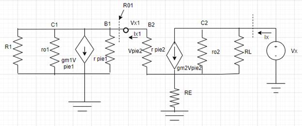
The small-signal equivalent circuit of BJT amplifier is as shown,
Apply KCL at base terminal of
Hybrid parameters p,
Substitute
Now rearrange the equation for output resistance
Expression for output resistance
Substitute equation (3) in equation (2)
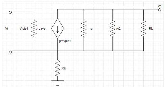
Now the small-signal equivalent circuit is modified for output resistance as shown,
Apply KVL for input voltage at above circuit,
Expression for hybrid parameter.
Put
Rearrange the equation for output resistance,
Consider
Substitute the value of equation (10) in (9)
Conclusion:
(b)
To find:An expression for small-signal voltage gain.
Answer to Problem 10.83P
Explanation of Solution
Given:
The given circuit is,
Calculation:
The small-signal equivalent circuit of BJT amplifier is as shown,
Apply KCL at base terminal of
Hybrid parameters p ,
Substitute
Now rearrange the equation for output resistance
Expression for output resistance
Substitute equation (3) in equation (2)
Now the small-signal equivalent circuit is modified for output resistance as shown, 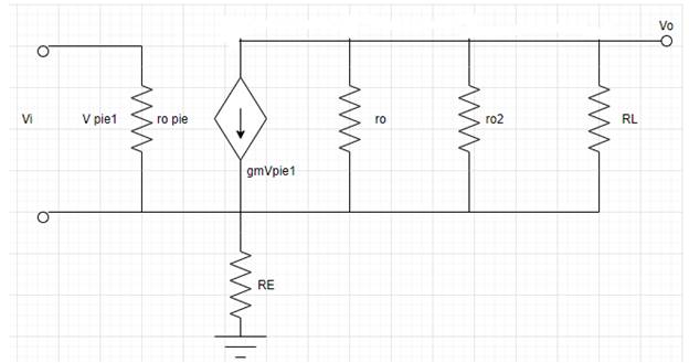
Apply KVL for input voltage at above circuit,
Expression for hybrid parameter.
Put
Rearrange the equation for output resistance,
Consider
Substitute the value of equation 10 in equation 9,
Now derive an expression for output voltage.
Input voltage will be,
Put
It is known that ,
The small-signal voltage gain derived expression is,
Conclusion:
Want to see more full solutions like this?
Chapter 10 Solutions
Microelectronics: Circuit Analysis and Design


- Please answer correctly and as soon as possible. I'll give upvote. Thank you. In the common emitter amplifier given, R1=50Ω, R2=1kΩ and CL=1pF. Determine the quiescent collector current, ICQ, needed such that the unity gain frequency, fu, is equal to 2.4 GHz. Show the complete solution and state all assumptions. The BJT parameters are as follows: β→∞,VA→∞, and Cπ=50 femtofarad (fF). Ignore all other parasitic capacitances and use VT=26mV.arrow_forward(a) What is the output current IO in the circuit as shown if −VEE = −15 V and R = 15ohm ?Assume that the BJT is in the forward-active reregionand βF = 30. (b) What is the voltage at theoutput of the operational amplifier if the saturationcurrent IS of the BJT is 10−13 A? (c) Whatis the minimum voltage VCC needed for forwardactiveregion operation of the bipolar transistor?(d) Find the power dissipation rating of the resistorR. How much power is dissipated in thetransistor if VCC = 15 V?arrow_forwardThe common-emitter amplifier given in the figure in the circuit, Vcc=9V, R1=27kΩ, R2=15kΩ, RE=1.2kΩ and RC=2.2kΩ. Transistor β=100 has value. a-) If it has values of Rsig=10kΩ and RL=2kΩ Calculate the IE of the amplifier. b-) For small signal analysis of transistor Find the value of Rin by deriving the π-model c-) Calculate vo/vsig and io/ii.arrow_forward
- A MOSFET common-source amplifier must amplify a sinusoidal ac signal with a peak amplitude of 0.4 V. What is the minimum value of VGS −VT Nfor the transistor? If a voltage gain of 26 dB is required, what is the minimum power supply voltage?arrow_forwardwhat is the Q point of the BJT(Vceq) between 0V and Vcc that maximizes the output voltage swing of a sinusoidal voltage. explain whyarrow_forwardDerive the expression for the following in terms ONLY of the small signalparameters and the given circuit components from the hybrid-pi model (Neglect the effect of the BJT’s small signal output resistancero):a.) RINb.) Gmc.) ROUTarrow_forward
- Explain the high frequency response of CS MOSFET Amplifier with proper equation. Discuss the effect of parasitic capacitances.arrow_forwardConsider below single-stage BJT amplifier circuit.arrow_forwardDiscuss and explain all capacitive reactances present in a BJT amplifier when frequency of the input signal isoutside of Midrange Region.arrow_forward
- What type of bias circuit can be used for the BJT amplifiers? Can the same type of bias circuit be configured as different types of BJT amplifier? Briefly answer.arrow_forwardIf RF = 50kΩ, R1 = 500kΩ and signal input is 15mV peak in a non-inverting operational amplifier, what will be the Vout value?arrow_forwardIn order to express the effect of the internal capacitors of BJT and the high frequency reception, the current gain expression depending on the frequency (Figure b) (hfe) is used in the case of collector emitter short circuit, voltage source connected at base end and emitter grounded (Figure la).. The catalog information of the 2N2222 transistor is given in Figure Ic. In the catalogue, when Ic=20 mA, it is seen as fT=250 MHz. a) Find the total capacitor effect for the case where gm> > wCμ. (Cpi) + (Cμ) = ?pFarrow_forward
 Introductory Circuit Analysis (13th Edition)Electrical EngineeringISBN:9780133923605Author:Robert L. BoylestadPublisher:PEARSON
 Delmar's Standard Textbook Of ElectricityElectrical EngineeringISBN:9781337900348Author:Stephen L. HermanPublisher:Cengage Learning
 Programmable Logic ControllersElectrical EngineeringISBN:9780073373843Author:Frank D. PetruzellaPublisher:McGraw-Hill Education
 Fundamentals of Electric CircuitsElectrical EngineeringISBN:9780078028229Author:Charles K Alexander, Matthew SadikuPublisher:McGraw-Hill Education
 Electric Circuits. (11th Edition)Electrical EngineeringISBN:9780134746968Author:James W. Nilsson, Susan RiedelPublisher:PEARSON
 Engineering ElectromagneticsElectrical EngineeringISBN:9780078028151Author:Hayt, William H. (william Hart), Jr, BUCK, John A.Publisher:Mcgraw-hill Education,