
Videos
Design a bipolar cascode amplifier with a cascode active load similar tothat in Figure P10.89 except the amplifying transistors are to be pnp andthe load transistors are to be npn. Bias the circuit at
The design of a circuit for a given specifications.
To find: The small-signal voltage gain
Answer to Problem D10.90P
The design is shown in Figure 2.
Explanation of Solution
Given:
Calculation:
The given circuit is,
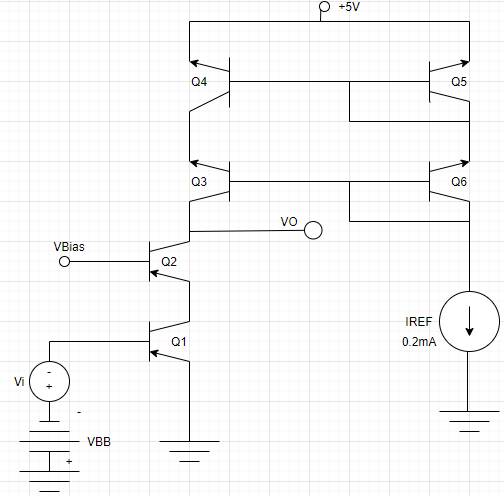
Figure 1
The equivalent designed circuit for active load amplifier is as shown,
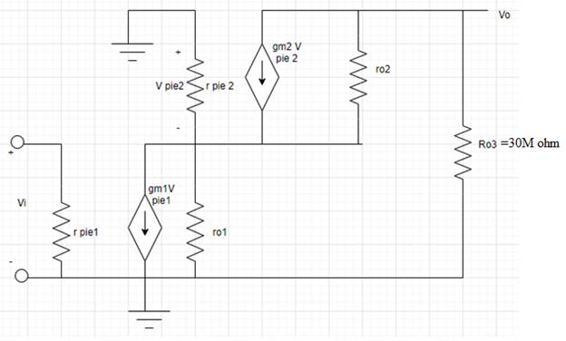
Figure 2
The expression for input voltage
Now expression for output resistance is,
Put equation (3) in equation (2).
Consider
Now expression for hybrid resistor parameter.
Now output voltage will be,
Consider
Put value from equation (8) to equation (6).
Put
Now
Substitute the value for
Now
Substitute the derived values in equation (10).
Want to see more full solutions like this?
Chapter 10 Solutions
Microelectronics: Circuit Analysis and Design


- (a) Does the MOSFET as shown remain in the active region of operation during the full-output signal swing? (b) If the dc drain current of the MOSFET in the active region is given by ID = (Kn/2)(VGS − VTN)2, what are the values of the parameter Kn and threshold voltage VTN for the transistor shown? (c) Express the amplifier voltage given in dB.arrow_forwardFor each transistor shown in Figure P10.1,determine whether the BE and BC junctions areforward- or reverse-biased, and determine theoperating region.arrow_forwardA MOSFET common-source amplifier must amplify a sinusoidal ac signal with a peak amplitude of 0.4 V. What is the minimum value of VGS −VT Nfor the transistor? If a voltage gain of 26 dB is required, what is the minimum power supply voltage?arrow_forward
- Vs=100 mV peak-to-peak, 1 kHz sine signal, Kn=0.4mA/v^2 ,Vt=1V , λ=0.01V^-1 Make the DC analysis of the above given mosfet amplifier circuit. Simulation to tableWrite down the measured values and mathematical calculation results. (The valueswith the units.)DC Parameters ,Measured value ,Calculated ValueVGETCVGSVDVDSIDb. Draw the small signal model for the AC analysis of the circuit. Find the gm, ro, Av values.c. Show the Vs input signal and the Vo output signal of the circuit on the oscilloscope. Volt/div of channels andSpecify time/div values.arrow_forwardGiven the circuit of Figure P10.5, determine theemitter current and the collector-base voltage. Assumethe BJT has Vγ = 0.6 V.arrow_forwardIn the common-emitter amplifier circuit shown in the figure, Vcc=9V, R1=27kΩ, R2=15kΩ, RE=1.2kΩ and RC=2.2kΩ. The transistor has β=100.a-) If Rsig=10kΩ and RL=2kΩ, calculate the IE value of the amplifier.b-) For small signal analysis of the transistor, find the value of Rin by deriving the π-modelc-) Calculate vo/vsig and io/ii.arrow_forward
- In the common emitter amplifier, R1 = 50Ω, R2 = 1kΩ, and CL=1 pF. Determine the quiescent collector current, ICQ, needed such that the unity gain frequency, fu, = 1 GHz. Show your complete solution and state all your assumptions.arrow_forward(a) What are the Q-points for the transistors in the amplifier as shown if VCC = 15 V, VEE = 15 V, IEE = 400 μA, βF = 100, REE = 270 kΩ,RC =47 kΩ, VA=∞, and βF =100? (b) What are the differential-mode gain, common-mode gain, CMRR, and differential-mode and common-modeinput and output resistances? (c) Repeat part (b) for VA = 50 V.arrow_forwardOperational Amplifiers Show solution to 6 & 7 pls??Thanks!arrow_forward
- The multistage amplifier circuit of Figure Q.2(b) have the following parameters:Q1 and Q2 : β = 200, VBE = 0.7 V, VT = 26 mV , VA = ∞Given that ICQ1 = 2 mA and VCEQ1 = 2 V. (i) Determine the value for RB4. List the assumption/approximation made in the analysis.(ii) Sketch and label the small-signal hybrid-π equivalent circuit at midbandfrequency range.(iii) Calculate the small signal hybrid-π model parameters: gm and rπ for Q1 and Q2. Then, determine Zi2 and Zo.arrow_forward(a) What is the output current IO in the circuit as shown if −VEE = −15 V and R = 15ohm ?Assume that the BJT is in the forward-active reregionand βF = 30. (b) What is the voltage at theoutput of the operational amplifier if the saturationcurrent IS of the BJT is 10−13 A? (c) Whatis the minimum voltage VCC needed for forwardactiveregion operation of the bipolar transistor?(d) Find the power dissipation rating of the resistorR. How much power is dissipated in thetransistor if VCC = 15 V?arrow_forwardWhat is the simple operational amplifier circuit for a constant current source? How does one set the Value of the current?arrow_forward
 EBK ELECTRICAL WIRING RESIDENTIALElectrical EngineeringISBN:9781337516549Author:SimmonsPublisher:CENGAGE LEARNING - CONSIGNMENT