
Videos
a.
The small-signal voltage gain
a.
Answer to Problem 11.84P
Explanation of Solution
Given:
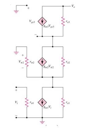
The given circuit is,
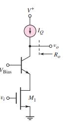
The two amplifying transistors
Calculation:
Consider the given figure,
Now find trans-conductance,
Now calculate
Now consider small-signal equivalent circuit,
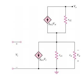
Apply nodal method at node
Now apply nodal method at node
Now consider,
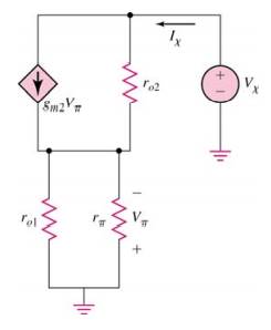
Find
Apply nodal analysis at node
Hence,
b.
The small-signal voltage gain
b.
Answer to Problem 11.84P
Explanation of Solution
Given:
The given circuit is,
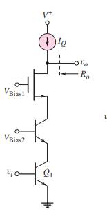
The two amplifying transistors
Calculation:
Consider the given figure,
Now find trans-conductance,
Now,
Now consider circuit,
Apply nodal at top part of the circuit,
Apply nodal at middle part of the circuit,
Find
Apply nodal analysis at node
Hence,
Want to see more full solutions like this?
Chapter 11 Solutions
Microelectronics: Circuit Analysis and Design


- What is the voltage gain of the common-emitter amplifier as shown? Assume βF = 135, VCC = VEE = 10 V, R1 = 20 kΩ, R2 = 62 kΩ,RC = 13 kΩ, and RE = 3.9 kΩ.arrow_forwardIf RB=12KΩ, RC=150Ω, VBB=7V, VCC=18V determine the IB, IC, IE and collector – emitter voltage in the circuit given below. The transistor has a gain (β) =150. Assume forward voltage drop of the BE junction is 0.7 V (Fig Q2 (d))arrow_forwardDetermine Vce for the given transistor configuration with the given parameters: Vcc = 17 V, Rc= 15,217 ohm, Rb= 11,473 ohm, Re 17,553 ohm, Vee -12 V and current gain = 147. Consider Ic to be approximately the same as Ie.arrow_forward
- Consider a CE circuit, where trans-conductance is 50mΩ-1, diffusion capacitance is 100 pF, transition capacitance is 3 pF. IB = 20μA. Given base emitter dynamic resistance, rbe = 1000 Ω, input VI is 20*sin(107t). What is the short circuit current gain?arrow_forward1) Find the operating point of the transistor by drawing the load line of the BJT transistor circuit given below. Calculate the voltage values VE and VC. (β = 100, VBE = 0.7 V, R1 = 10 KΩ, RC = 4.7 KΩ, RE = 3.3 KΩ, VCC = 10 V, VEE = - 4 V)arrow_forwardFor the NMOSFET in the circuit below, K = 2.00mA/V2, VTHN = 1.00V, l = 0.05V-1, and VIN = 3.50V. a. Solve for IDS and VOUT and verify any assumptions you made. b. Calculate the small signal gain of the circuit, vout / vin .arrow_forward
- Given VTH=1.2 and k=0.5mA/V2, determine the following a) The value of ID, VGS and VDS b) Mode of operation of the MOSFET. (Verify this answer)arrow_forwardProblem: Fx=(AB+CD+EF+G)' a. Draw its equivalent transistor circuit. b. Determine if the function has an Euler's path. please draw the equivalent Euler's path. C. Whether the circuit has a Euler's path or not, draw the stick diagram.arrow_forward4) By drawing the small signal model of the circuit given below, we can determine the total voltage and current gain values of the circuit, without the bypass capacitor on and without the bypass capacitor. Calculate separately for the two cases as it will be in the circuit (connected to the emitter end of the transistor). (β = 100, rS = 600 Ω, R1 = 27 KΩ, R2 = 4.7 KΩ, RC = 3.3 KΩ, RE = 680 Ω, RL= 15 KΩ, VCC = 10 V)arrow_forward
- Please help with this homework problem. The topic is Bipolar Junction Transistors (BJTs). I'm having a difficult time understanding how to replace the transistor with the small-signal equivalent.arrow_forwardDraw, Illustrate and label your schematic diagram before solving the problem. 1) Given a Fixed-Biased transistor circuit with Beta DC is 200 , voltage at common collector is +22v ,base supply voltage is +11V, Base resistor is 47kOhms , collector resistor is 390 ohms ,Voltage at Base-emitter junction is 0.7v. Determine the Q-point of collector current and Voltage at collector-emitter junction. These might be help as a guide to solve the problem.arrow_forwardIn the circuit shown, RL = 2 k , VCC =15 V, and −VEE = −15 V. (a) What is the maximumvalue of RE that can be used if vO is to reach−12.5 V? (b) What is the emitter current of Q1when vO = +12.5 V?arrow_forward
 Introductory Circuit Analysis (13th Edition)Electrical EngineeringISBN:9780133923605Author:Robert L. BoylestadPublisher:PEARSON
 Delmar's Standard Textbook Of ElectricityElectrical EngineeringISBN:9781337900348Author:Stephen L. HermanPublisher:Cengage Learning
 Programmable Logic ControllersElectrical EngineeringISBN:9780073373843Author:Frank D. PetruzellaPublisher:McGraw-Hill Education
 Fundamentals of Electric CircuitsElectrical EngineeringISBN:9780078028229Author:Charles K Alexander, Matthew SadikuPublisher:McGraw-Hill Education
 Electric Circuits. (11th Edition)Electrical EngineeringISBN:9780134746968Author:James W. Nilsson, Susan RiedelPublisher:PEARSON
 Engineering ElectromagneticsElectrical EngineeringISBN:9780078028151Author:Hayt, William H. (william Hart), Jr, BUCK, John A.Publisher:Mcgraw-hill Education,