
a.
The differential-mode voltage gain
a.
Answer to Problem 11.92P
Explanation of Solution
Given:
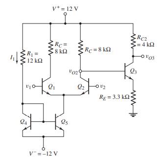
The given circuit is,
Calculation:
Consider the given figure,
The voltage
The input resistance of the CE amplifier is,
Now calculate the output resistance,
Now calculate
Hence,
b.
The output voltage
To compare: The obtained result with the ideal output.
b.
Answer to Problem 11.92P
The output voltage obtained for ideal case is greater than the actual result obtained.
Explanation of Solution
Given:
The given circuit is,
Calculation:
Consider the given voltage,
The differential input voltage will be,
Now calculate output voltage,
Now calculate output voltage for ideal case,
Put
Hence,
It is observed that both the values are slightly different. The output voltage obtained for ideal case is greater than the actual result obtained.
c.
The differential-mode and common-mode input resistances.
c.
Answer to Problem 11.92P
Explanation of Solution
Given:
The given circuit is,

Calculation:
Let calculatethe differential-mode input resistances,
The common-mode input resistances will be,
Hence,
Want to see more full solutions like this?
Chapter 11 Solutions
Microelectronics: Circuit Analysis and Design

- Q.4/ Refer to the class AB power amplifier shown below:a. Determine the dc parameters VB(Q1), VB(Q2), ICQ, VCEQ(Q1), VCEQ(Q2).b. For the 5Vrms input, determine the power delivered to the load resistor.c. Determine the approximate input resistance seen by the signal source if ac=100arrow_forwardThe ac equivalent circuit for an amplifier is shown. Assume the capacitors have infinite value, RI =750Ω, RB =100 kΩ, RC =100 kΩ, and R3 =100 kΩ. Calculate the input resistance and output resistance for the amplifier if the BJT Q-point is (75 μA, 10 V). Assume βo =100 and VA =75 V.arrow_forwardConsider the common-source amplifier shown in Figure P11.50. The NMOS transistor has KP=50 μA/V2, L=5 μm, W=500 μm, Vto=1 V and rd=∞.a. Determine the values of IDQ, VDSQ and gm. b. Compute the voltage gain, input resistance, and output resistance, assuming that the coupling capacitors are short circuits for the ac signal. Repeat Problem P11.50 for an NMOS transistor having KP=50 μA/V2, W=600 μm, L=20 μm, Vto=2 V and rd=∞. Compare the gain with that attained in Problem P11.50.arrow_forward
- Consider the circuit. The transistor has a parameter β that varies between 50 and 200. The operation of the circuit and the electrical variables at the end points must be known. end points. Calculate the following for β = 50 and β = 200. a) lE, VE and VB (DC analysis). b) The input resistance Rin (small signal analysis). c) Voltage gain V0/ Vsig (Small Signal Analysisarrow_forwardFor the class B output stage of Figure 2, let VCC = 6 V and RL = 4Ω. If the output is a sinusoidal with 4.5V peak amplitude, find; (a) The output power. (b) The average power drawn from each supply/ (c) The power efficiency obtained at this output voltage. (d) The maximum power that each transistor must be capable of dissipating safely.arrow_forwardFor the cascaded amplifier of the figure below, calculate the input impedance of the first stage, output impedance of the second stage, total voltage gain, and the output voltage if Vs= 1mV.arrow_forward
- Amplifier circuit is show below has a single ac input and one ac output. Assuming 2N2222 transistor: Construct the T-model of the transistor with all parameters labelled and evaluated. Assume room temperature. Draw a complete small signal circuit model, then find the voltage gain. Explain two characteristics of this amplifier. Calculate the current gain, the input resistance, and the output resistance.arrow_forwardAmplifier circuit is show below has a single ac input and one ac output. Assuming 2N2222 transistor: 1- Determine the Q point, then illustrate it on the transistor I-V characteristic curves. 2- Is the transistor in the active region? Explain thoroughly. 3- Construct the T-model of the transistor with all parameters labelled and evaluated. Assume room temperature. 4- Draw a complete small signal circuit model, then find the voltage gain. Explain two characteristics of this amplifier. 5- Calculate the current gain, the input resistance, and the output resistance.arrow_forwardConsider the amplifier in the figure given below, where VA = 50 V, VCC = 20 V, VEE = 20 V, IEE = 350 μA, βF = 120, REE = 320 kΩ, and RC = 72 kΩ. What are the differential-mode input and output resistances of the given amplifier?arrow_forward
- Topic: Field Effect Transistor Given the FET Amplifier circuit. Answer the question asked in each letter. a. Transconductance Gain (gm) b. Drain Resistor (RD) c. Input Impedance (Zi) d. Output Impedance (Zo) e. Voltage Gain (Av) f. What is the AC configuration of the amplifier?common source, common gate, common drain, or source bias?arrow_forwardGiven the differential amplifier circuit below. Determine the following: emitter current, differential mode voltage gain, common mode voltage gain and CMRR.arrow_forwardKnowing the equation of collector current IC for the transistor amplifier circuit, please calculate the current and voltage stabilization factors. Rc=2000ohm Re=500ohm Rb=500ohm Rb=1000ohm Beta0=200arrow_forward
 Introductory Circuit Analysis (13th Edition)Electrical EngineeringISBN:9780133923605Author:Robert L. BoylestadPublisher:PEARSON
 Delmar's Standard Textbook Of ElectricityElectrical EngineeringISBN:9781337900348Author:Stephen L. HermanPublisher:Cengage Learning
 Programmable Logic ControllersElectrical EngineeringISBN:9780073373843Author:Frank D. PetruzellaPublisher:McGraw-Hill Education
 Fundamentals of Electric CircuitsElectrical EngineeringISBN:9780078028229Author:Charles K Alexander, Matthew SadikuPublisher:McGraw-Hill Education
 Electric Circuits. (11th Edition)Electrical EngineeringISBN:9780134746968Author:James W. Nilsson, Susan RiedelPublisher:PEARSON
 Engineering ElectromagneticsElectrical EngineeringISBN:9780078028151Author:Hayt, William H. (william Hart), Jr, BUCK, John A.Publisher:Mcgraw-hill Education,