
Videos
The transistor parameters for the circuit in Figure
a.
To design: The circuit for the given parameters.
Answer to Problem D11.105DP
The design of the given circuit is shown in Figure 2.
Explanation of Solution
Given:
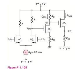
The given circuit is shown below.
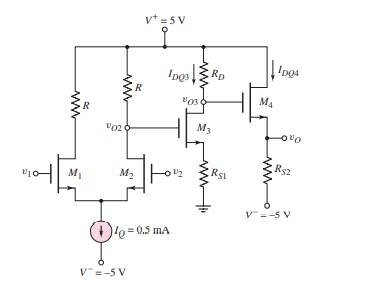
Figure 1
Calculation:
Consider the differential circuit part,
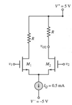
The circuit is symmetrical because currents divides between both MOSFETs. Now consider one by one part of the circuit.
Now find
Now find
Now calculate
Now the design is shown below.
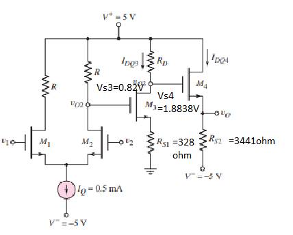
Figure 2
b.
The differential-mode gains.
Answer to Problem D11.105DP
Explanation of Solution
Given:
The given circuit is shown below.

Calculation:
Consider the
Put the calculated values in above equation,
Now,
Now find,
Put the values in
c.
The common-mode voltage gains and
Answer to Problem D11.105DP
Explanation of Solution
Given:
The given circuit is shown below.

Calculation:
Consider the
Hence the
Want to see more full solutions like this?
Chapter 11 Solutions
Microelectronics: Circuit Analysis and Design


- The ac equivalent circuit for an amplifier is shown. Assume the capacitors have infinite value, RI = 100 kΩ, RG = 6.8MΩ, RD = 50 kΩ, and R3 = 120 kΩ. Calculate the voltage gain for the amplifier if the MOSFET Q-point is (100 μA, 5 V). Assume Kn = 450 μA/V2 and λ = 0.02 V−1.arrow_forwardWhat is the voltage gain (Av) of the circuit when = 100, r0 = 40 kΩ, RB = 360 kΩ, RC = 3.3 kΩ, RE = 220 Ω, Rs = 15 kΩ and RL = 379 kΩ? NOTE-1: The output impedance r0 of the transistor will be taken into account in the calculations. NOTE-2: Capacitors are negligible at mid-band frequency.arrow_forwardSince Vcc = 25 V, Vi = 31 mV, RB = 470 kΩ, RC = 3.2 kΩ, RE1 = 470 Ω, RE2 = 1.2 kΩ, RL = 40.5 kΩ and β = 110 in the circuit in the figure, the output voltage (Vo Find the value of ). NOTE-1: Capacitors are negligible at mid-band frequency. NOTE-2: The output impedance (r0) of the transistor will be neglected.arrow_forward
- If the multistage amplifier is driven by a 1 μV source and the last stage is loaded with an RL = 20 kΩ, determine the ac emitter resistor, re, for each stage. Given: R1 = 33 kΩ, R2 = 8.2 kΩ, RC = 3.3 kΩ, RE = 1 kΩ, Beta = 175arrow_forwardDraw the DC circuit: b)DC computations: Compute the DC collector current of each transistor. I_C 1 = ________________________ mA I_C 2= ________________________ Calculations: c)Draw the AC circuit and compute gm, r_pi for the system. g_m 1= _______________________ mA/V r_pi 1 = _______________________ kohms g_m 2= _______________________ mA/V r_pi 2 = _______________________ kohms AC circuit: Calculations: d)Compute the gain A_v=Vo/Vi at the operational band (for sufficiently high frequency) Gain = A_v = ______________________________ Computations:arrow_forwardSince Vcc = 25 V, Vi = 2 mV, RB = 470 kΩ, RC = 1.5 kΩ, RE1 = 470 Ω, RE2 = 1.2 kΩ, RL = 42 kΩ and β = 110 in the circuit in the figure, the value of the output voltage (Vo) find it. NOTE-1: Capacitors are negligible at mid-band frequency. NOTE-2: The output impedance (r0) of the transistor will be neglected.arrow_forward
- The ac equivalent circuit for an amplifier is shown. Assume the capacitors have infinite value, RI =750Ω, RB =100 kΩ, RC =100 kΩ, and R3 =100 kΩ. Calculate the input resistance and output resistance for the amplifier if the BJT Q-point is (75 μA, 10 V). Assume βo =100 and VA =75 V.arrow_forwardVcc=25V , Vi=35mV , RB =470kΩ , RC=2,6kΩ , RE1=470Ω , RE2=1.2kΩ , RL=16.8kΩ , β=110 Find the output voltage V0 = ? Note1=Capacitors are negligible at mid-band frequency. Note2 0 The output impedance (r0) of the transistor will be neglected.arrow_forwardIn the circuit given in the figure, what is the voltage gain (Av) of the circuit when = 100, r0 = 40 kΩ, RB = 360 kΩ, RC = 3.3 kΩ, RE = 220 Ω, Rs = 15 kΩ and RL = 166 kΩ?NOTE-1: The output impedance r0 of the transistor will be taken into the calculations.NOTE-2: Capacitors are negligible at mid-band frequency.arrow_forward
- The ac equivalent circuit for an amplifier is shown. Assume the capacitors have infinite value, RI = 100 kΩ, RG = 10 MΩ, RD = 560 kΩ, and R3 = 1.5 MΩ. Calculate the voltage gain for the amplifier if the MOSFETQ-point is (10 μA, 5 V). Assume Kn = 100 μA/V2 and λ = 0.02 V−1.arrow_forward1. The high frequency response of an RC coupled amplifier depends on: a) The input coupling capacitors b) The midrange voltage gain The bypass capacitor d) The output coupling capacitors 2. IM the peak output voltage of an amplifier at the critical frequency is 20 V. the output voltage at midrange is: a) 17 V b) 23 V c) 14.14 V d) 28.3V 3. The low frequency response of RC coupled BJT amplifier depends on 1.) The bypass capacitor b) l'he input and output capacitors c) The input coupling capacitor d) All capacitors in the circuit +. The input Miller capacitance of a BJT amplifier depends partly on: a) Inpui coupling capacitor b) The voltage gain at lower critical frequency ) The internal capacitances of the transistor d) the bypass capacitor 5 When the frequency of an amplifier is reduced linearly from 100 kHz to 1 kHz. the gain of the amplilier is reduced by 12 213. then the roll-off rate is: a)-12 dB/octave b) - 12 dB/ decade c) -6 dB/ decade d) -6 dB/octave 6. A multistage amplifier…arrow_forwardIn the circuit below, it is given as RE=1kΩ, RC=5kΩ, VEE=2V, VCC=8V. Parameters of the transistor in the circuit are given as aac =0.98,β0=100. Calculate the input and output impedances of the circuit and the current and voltage gains for medium frequencies.arrow_forward
 Introductory Circuit Analysis (13th Edition)Electrical EngineeringISBN:9780133923605Author:Robert L. BoylestadPublisher:PEARSON
 Delmar's Standard Textbook Of ElectricityElectrical EngineeringISBN:9781337900348Author:Stephen L. HermanPublisher:Cengage Learning
 Programmable Logic ControllersElectrical EngineeringISBN:9780073373843Author:Frank D. PetruzellaPublisher:McGraw-Hill Education
 Fundamentals of Electric CircuitsElectrical EngineeringISBN:9780078028229Author:Charles K Alexander, Matthew SadikuPublisher:McGraw-Hill Education
 Electric Circuits. (11th Edition)Electrical EngineeringISBN:9780134746968Author:James W. Nilsson, Susan RiedelPublisher:PEARSON
 Engineering ElectromagneticsElectrical EngineeringISBN:9780078028151Author:Hayt, William H. (william Hart), Jr, BUCK, John A.Publisher:Mcgraw-hill Education,