
Videos
Consider the series-shunt feedback circuit in Figure
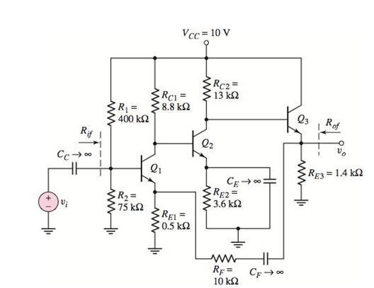
Figure P12.37
(a)
The small signal parameter for
Answer to Problem 12.37P
The trans-conductance of the first transistor
Explanation of Solution
Given:
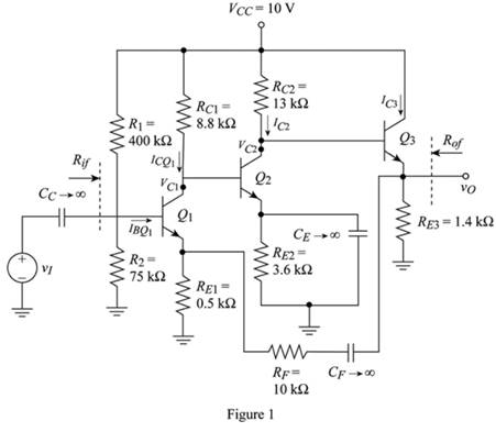
The given circuit is shown in Figure 1
Calculation:
The value of the Thevenin voltage is given by,
The expression for the equivalent resistance is given by,
The expression for the current
Substitute
The expression to determine the value of the collector current
Substitute
The expression for the collector voltage
Substitute
The expression for the value of the current
Substitute
The expression for the collector voltage
Substitute
The expression for the value of the current
Substitute
The expression for the small signal input resistance is given by,
Substitute
The expression for the trans-conductance of the first transistor is given by,
Substitute
The expression for the small signal input resistance is given by,
Substitute
The expression for the trans-conductance of the first transistor is given by,
Substitute
The expression for the small signal input resistance is given by,
Substitute
The expression for the trans-conductance of the first transistor is given by,
Substitute
Conclusion:
Therefore, the trans-conductance of the first transistor
(b)
The value of the small signal voltage gain
Answer to Problem 12.37P
The value of small signal voltage gain is 20.7.
Explanation of Solution
Given:
The given circuit is shown in Figure 1

Calculation:
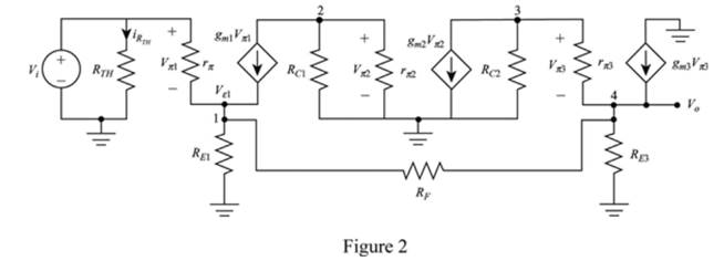
Mark the values and draw the small signal equivalent circuit.
The required diagram is shown in Figure 2
The expression for the input voltage
Apply KCL at the node 1
Substitute
Substitute
Apply KCL at node 2.
Substitute
Apply KCL at the node 3
Substitute
Substitute
Apply KCL at the node 4
Substitute
Substitute
Substitute
Substitute
Conclusion:
Therefore, the value of small signal voltage gain is 20.7.
(c)
The value of the resistance
Answer to Problem 12.37P
The value of the input resistance is
Explanation of Solution
Given:
The given circuit is shown in Figure 1

Calculation:
The expression to determine the value of the current
Substitute
The value of
Substitute
The expression for the current
Substitute
The expression for the input current
Substitute
Conclusion:
Therefore, the value of the input resistance is
(d)
The value of the resistance
Answer to Problem 12.37P
The value of the output resistance is
Explanation of Solution
Given:
The given circuit is shown in Figure 1

Calculation:
Consider the equation (1).
Substitute
The equation for
Substitute
Consider the equation given,
Substitute
Substitute
Conclusion:
Therefore, the value of the output resistance is
Want to see more full solutions like this?
Chapter 12 Solutions
Microelectronics: Circuit Analysis and Design


- Discuss the distinction between open-loop gain and closed-loop gain.arrow_forwardWhat are the advantages of positive feedback amplifier?arrow_forwardA unity feedback system with open-loop transfer function given as:?(?) = ??. ?(? + ?)(? + ?)(? + ??)without affecting its operating point (−1.54 ∓ ??2.66) appreciably a- Design a suitable compensator to drive the step response error to zero.b- Design a suitable compensator to reduce step error by factor of 5.arrow_forward
- Using Routh-criterion investigate the stability of a unity feedback control system whose open loop transfer function is given by, G(s) = (e ^ (- s * T))/(s(s + 2))arrow_forwarda) reduce the block diagram with transfer functions into a unity feedback system configuration as shown in Figure 1 b) Using Routh Hurwitz criterion, do stability analysis to the system with K=1.arrow_forwardDiscuss the difference between the Current series negative feddback amplifier and voltage shunt feedback amplifier.arrow_forward
- Consider the unit feedback control system with the following transfer function: (image shown). Draw the Nyquist diagram of G(s) and examine the closed-loop stability of the system.arrow_forwardLoop gain analysis in a feedback system applies for __________. Option (1) small-signal perturbations Option (2) large-signal perturbations Option (3) both large and small-signal perturbationsarrow_forwarddescribe the expression of sensitivity of C.L.T.F. wrt. feedback gain.arrow_forward
 Introductory Circuit Analysis (13th Edition)Electrical EngineeringISBN:9780133923605Author:Robert L. BoylestadPublisher:PEARSON
 Delmar's Standard Textbook Of ElectricityElectrical EngineeringISBN:9781337900348Author:Stephen L. HermanPublisher:Cengage Learning
 Programmable Logic ControllersElectrical EngineeringISBN:9780073373843Author:Frank D. PetruzellaPublisher:McGraw-Hill Education
 Fundamentals of Electric CircuitsElectrical EngineeringISBN:9780078028229Author:Charles K Alexander, Matthew SadikuPublisher:McGraw-Hill Education
 Electric Circuits. (11th Edition)Electrical EngineeringISBN:9780134746968Author:James W. Nilsson, Susan RiedelPublisher:PEARSON
 Engineering ElectromagneticsElectrical EngineeringISBN:9780078028151Author:Hayt, William H. (william Hart), Jr, BUCK, John A.Publisher:Mcgraw-hill Education,