Microelectronics: Circuit Analysis and Design
4th Edition
ISBN: 9780073380643
Author: Donald A. Neamen
Publisher: McGraw-Hill Companies, The
bartleby

Concept explainers

bartleby

Videos

Textbook Question
Book Icon
Chapter 12, Problem 12.50P

(a) Using the small-signal equivalent circuit in Figure 12.25 for the circuit in Figure 12.24 ( a ) , derive the expression for the small-signal current gain A i f = I o / I s . (b) Using the circuit parameters given in Figure 12.24 ( a ) and assuming transistor parameters h F E = 100 and V A = calculate the value of A i f . Compare this answer with the results of Example 12.9.

(a)

Expert Solution
Check Mark
To determine

To derive: The expression for the small signal current gain of the circuit.

Answer to Problem 12.50P

The value of the small signal current gain is { R F( 1 R B || R B2 ) g m1+( R F R s || R B1 || r π1 || R F )( 1 R B || R B2 )[( R F R s || R B1 || r π1 || R F )B1 R F ]RFB}1g m2[( R C2 + R L R C2 )]{( 1 r π2 + g m2){( 1 R 2 + g m2 )+D A( 1 R B || R B2 )+ g m1 }[( AB)1 R F ]} .

Explanation of Solution

Given:

The given circuit is shown in Figure 1.
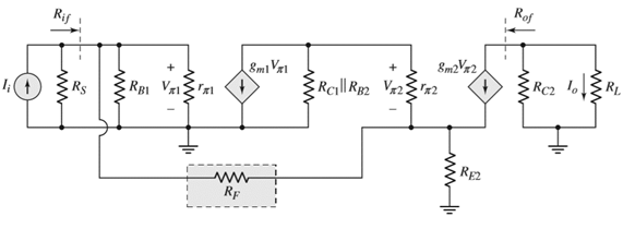
  Microelectronics: Circuit Analysis and Design, Chapter 12, Problem 12.50P , additional homework tip  1

Figure 1

Calculation:

Mark the nodes and redraw the circuit.

The given diagram is shown in Figure 2
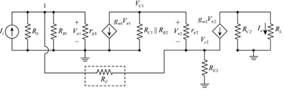
  Microelectronics: Circuit Analysis and Design, Chapter 12, Problem 12.50P , additional homework tip  2

Figure 2

By KCL the expression for the current Ii is given by,

  Ii=V π1Rs||R B1||r π1+V π1V e2RFVe2=Vπ1( R F R s || R B1 || r π1 || R F )IiRF

The expression for the node voltage is given by,

  VC1=Vπ2+Ve2

Apply KCL at node VC1 .

  gm1Vπ1+V C1R C1||R B2+V π2r π2=0gm1Vπ1+V π2+V e2R C1||R B2+V π2r π2=0gm1Vπ1+Vπ2(1 R C1 || R B2 || r π2 )+V e2R C12||R B2=0

Substitute Vπ1(RFRs||R B1||r π1||RF)IiRF for Ve2 in the above equation.

  gm1Vπ1+Vπ2(1 R C1 || R B2 || r π2 )+1R C12||R B2[Vπ1( R F R s || R B1 || r π1 || R F )IiRF]=0Vπ1=IiRF( 1 R C12 || R B2 )V π2( 1 R C || R B2 || r π2 )g m1+[( R F R s || R B1 || r π1 || R F )( 1 R C12 || R B2 )]

The expression for the output current is given by,

  IO=(g m2V π2)( R C2 R C2 + R L )Vπ2=IOg m2( R C2 + R L R C2 )

Apply KCL at node Ve2 .

  V π2r π2+gm2Vπ2=V e2R E2+V e2V π1RF(1 r π2 +g m2)Vπ2+V π1RF=(1 R E2 +1 R F )Ve2

Substitute Vπ1(RFRs||R B1||r π1||RF)IiRF for Ve2 in the above equation.

  (1 r π2 +g m2)Vπ2+V π1RF=(1 R E2 +1 R F )(V π1( R F R s || R B1 || r π1 || R F )IiRF)(1 r π2 +g m2)Vπ2+IiRF(1 R E2 +1 R F )=Vπ1{[( R F R s || R B1 || r π1 || R F )( 1 R E2 + 1 R F )]1 R F}

Substitute IiRF(1 R C12 || R B2 )Vπ2(1 R C || R B2 || r π2 )gm1+[( R F R s || R B1 || r π1 || R F )( 1 R C12 || R B2 )] for Vπ1 in the above equation.

  [( 1 r π2 + g m2)Vπ2+IiRF( 1 R E2 + 1 R F )]=[ I i R F( 1 R C1 || R B2 ) V π2( 1 R C || R B2 || r π2 )][gm1+[ ( R F R s || R B1 || r π1 || R F ) ( 1 R C12 || R B2 )]]{[( R F R s || R B1 || r π1 || R F )( 1 R E2 + 1 R F )]1RF}

Consider A=RFRs||RB1||rπ1||RF , B=1RE2+1RF , C=1RC1||RB2 and D=1RC1||RB2||rπ2 in the above equation. So the equation is,

   [ ( 1 r π2 + g m2 ) V π2 + I i R F B ]= [ I i R F C V π2 D ] [ g m1 +AC ] { AB 1 R F }

   V π2 { ( 1 r π2 + g m2 )+ D g m1 +AC [ AB 1 R F ] }= I i { R F C g m1 +AC [ AB 1 R F ] R F B }

   [ I O g m2 ( R C2 + R L R C2 ) ]{ ( 1 r π2 + g m2 )+ D g m1 +AC [ AB 1 R F ] }= I i { R F C g m1 +AC [ AB 1 R F ] R FB B }

   I O I i = { R F C g m1 +AC [ AB 1 R F ] R F B } 1 g m2 [ ( R C2 + R L R C2 ) ]{ { ( 1 r π2 + g m2 )+ D AC+ g m1 }[ ( AB ) 1 R F ] }

Thus, the expression for the small signal current gain is,

  Ai={ R FC g m1+AC[AB1 R F ]RFB}1g m2[( R C2 + R L R C2 )]{{( 1 r π2 + g m2 )+D AC+ g m1 }[( AB)1 R F ]} …….(1)

Conclusion:

Therefore, the value of the small signal current gain is { R F( 1 R B || R B2 ) g m1+( R F R s || R B1 || r π1 || R F )( 1 R B || R B2 )[( R F R s || R B1 || r π1 || R F )B1 R F ]RFB}1g m2[( R C2 + R L R C2 )]{( 1 r π2 + g m2){( 1 R 2 + g m2 )+D A( 1 R B || R B2 )+ g m1 }[( AB)1 R F ]} .

(b)

Expert Solution
Check Mark
To determine

The value of the gain Aif for the given specifications.

To compare: The obtained value with the given value of gain. and compare it to the value of 9.58.

Answer to Problem 12.50P

The value of the current gain is 9.58 and it is approximately equal to the given value of gain.

Explanation of Solution

Given:

The given circuit is shown below.

  Microelectronics: Circuit Analysis and Design, Chapter 12, Problem 12.50P , additional homework tip  3

The given value of gain is 9.58.

Also, the values are:

  hFE=100VA=

Calculation:

The expression to determine the value of the resistance RB1 is given by,

  RB1=( 80kΩ)( 20kΩ)( 80kΩ)+( 20kΩ)=16kΩ

The expression for the value of the voltage VTH1 is given by,

  VTH1=VCC( R 2 R 2 + R 1 )=10V( 20kΩ 100kΩ)=2V

The expression to determine the value of the current IB1 is given by,

  IBQ1=VTH1VBE(on)RB1+(h fe+1)RE1

Substitute 2V for VTH1 , 0.7V for VBE , 16kΩ for RB1 and 1kΩ for RE1 in the above equation.

  IBQ1=2V0.7V16kΩ+( 100+1)1kΩ=0.0111mA \

The value of the current ICQ1 is calculated as,

  ICQ1=hFEIBQ1

Substitute 100 for hFE and 0.0111mA for IBQ1 in the above equation.

  ICQ1=(100)(0.0111mA)=1.11mA

The expression to determine the value of the resistance RB2 is given by,

  RB2=R3||R4=( 85kΩ)( 15kΩ)( 85kΩ)+( 15kΩ)=12.75kΩ

The value of the Thevenin voltage is given by,

  VTH2=VCC( R 4 R 3 + R 4 )=(10V)( 15kΩ 15kΩ+85kΩ)=1.5V

The expression to determine the value of the current IB2 is given by,

  IBQ2=VTH2VBE(on)RB2+(h fe+1)RE2

Substitute 1.5V for VTH2 , 0.7V for VBE , 12.75kΩ for RB2 and 0.5kΩ for RE2 in the above equation.

  IBQ2=1.5V0.7V12.75kΩ+( 100+1)0.5kΩ=0.01265mA \

The value of the current ICQ2 is calculated as,

  ICQ2=hFEIBQ2

Substitute 100 for hFE and 0.01265mA for IBQ2 in the above equation.

  ICQ2=(100)(0.01265mA)=1.265mA

The expression to determine the transconductance of first transistor is calculated as,

  gm1=1.11mA0.026V=42.69mA/V

The expression to determine the transconductance of second transistor is calculated as,

  gm1=1.265mA0.026V=48.65mA/V

The value of the small signal input resistance is calculated as,

  rπ1=h FEg m1=10042.69mA/V=2.34kΩ

The value of the small signal input resistance is calculated as,

  rπ2=h FEg m2=10048.65mA/V=2.06kΩ

The value of A is calculated as,

  A=RFRs||R B1||r π1||RFRFR B1||r π1||RF=10kΩ16kΩ||2.34kΩ||10kΩ=5.896

The value of B is calculated as,

  B=1R E2+1RF=10.5kΩ+110kΩ=2.1m

The value of C is calculated as,

  C=1RB||RB2

The value of D is calculated as,

  D=1RC1||RB2||rπ2

Substitute 1.7289kΩ for RC1||RB2 and 2.06kΩ for rπ in the above equation.

  D=11.7289kΩ||2.06kΩ=1.0627m , 4kΩ

Substitute 10kΩ for RF , 42.69mA/V for gm1 , 48.65mA/V for gm2 , 4kΩ for RC2 , 4kΩ for RE , 2.06kΩ for rπ2 , 5.896 for A , 2.1m for B , 0.5784m for C and 1.0672m for D in equation (1).

  Ai={ ( 10kΩ )( 0.5784m ) ( 42.69 mA V )+[ ( 5.896 ) ( 0.5784m ) ][ ( 5.896 )( 2.1m ) 1 ( 10kΩ ) ][ ( 10kΩ ) ( 2.1m ) ]} 1 48.65 mA V [( ( 4kΩ )+( 4kΩ ) ( 4kΩ ) )]{ { ( 1 2.06kΩ +48.65 mA V ) + ( 1.0627m ) ( 5.896 )( 0.5784m )+42.69 mA V } [ ( ( 5.896 ) ( 2.1m ) ) 1 ( 10kΩ ) ] }=19.46( 0.0411)( 49.4174)=9.58122

The value of the current gain is 9.58122 and it is approximately equal to the given value of gain.

Want to see more full solutions like this?

Subscribe now to access step-by-step solutions to millions of textbook problems written by subject matter experts!
Students have asked these similar questions
For the 2 circuits shown above, βnpn = 100, βpnp = 50, VDO = 0.7 V, R2 = 150 kΩ, and RB = 12 kΩ Using the ac small-scale signal analysis, determine for each circuit: a) The voltage gain (Av = vout/vin) b) The input resistance (Rin) c) The output resistance (Rout)
Consider the circuit of Figure 12.7 on page 605. Assume that VCC=20 V, VBB=0.3 V, RB=40 kΩ, and RC=2 kΩ. The input signal is a 0.2-V-peak 1-kHz sinusoid given by vin(t)=0.2 sin(2000πt). The common-emitter characteristics for the transistor are shown in Figure P12.18. Determine the maximum, minimum, and Q-point values for vCE. What is the approximate voltage gain for this circuit? Why is the gain so small in magnitude?
Topic: Field Effect Transistor Given the FET Amplifier circuit. Answer the question asked in each letter. a. Transconductance Gain (gm) b. Drain Resistor (RD) c. Input Impedance (Zi) d. Output Impedance (Zo) e. Voltage Gain (Av) f. What is the AC configuration of the amplifier?common source, common gate, common drain, or source bias?

Chapter 12 Solutions

Microelectronics: Circuit Analysis and Design

Ch. 12 - Prob. 12.5TYUCh. 12 - Consider the noninverting op-amp circuit shown in...Ch. 12 - Design a feedback voltage amplifier to provide a...Ch. 12 - Prob. 12.6TYUCh. 12 - (a) Assume the transistor in the source-follower...Ch. 12 - Consider the common-base circuit in Figure...Ch. 12 - Design a feedback current amplifier to provide a...Ch. 12 - Prob. 12.8TYUCh. 12 - Prob. 12.9TYUCh. 12 - For the circuit in Figure 12.31, the transistor...Ch. 12 - Design a transconductance feedback amplifier with...Ch. 12 - Prob. 12.10TYUCh. 12 - Consider the circuit in Figure 12.39, with...Ch. 12 - Consider the BJT feedback circuit in Figure...Ch. 12 - Prob. 12.12TYUCh. 12 - Consider the circuit in Figure...Ch. 12 - Prob. 12.16EPCh. 12 - Prob. 12.17EPCh. 12 - Consider the circuit in Figure 12.44(a) with...Ch. 12 - Consider the circuit in Figure 12.16 with the...Ch. 12 - Prob. 12.18EPCh. 12 - Consider the loop gain function T(f)=(3000)(1+jf...Ch. 12 - Consider the loop gain function given in Exercise...Ch. 12 - Prob. 12.16TYUCh. 12 - Prob. 12.17TYUCh. 12 - Prob. 12.20EPCh. 12 - Prob. 12.21EPCh. 12 - Prob. 12.22EPCh. 12 - What are the two general types of feedback and...Ch. 12 - Prob. 2RQCh. 12 - Prob. 3RQCh. 12 - Prob. 4RQCh. 12 - Prob. 5RQCh. 12 - Prob. 6RQCh. 12 - Describe the series and shunt output connections...Ch. 12 - Describe the effect of a series or shunt input...Ch. 12 - Describe the effect of a series or shunt output...Ch. 12 - Consider a noninverting op-amp circuit. Describe...Ch. 12 - Prob. 11RQCh. 12 - What is the Nyquist stability criterion for a...Ch. 12 - Using Bode plots, describe the conditions of...Ch. 12 - Prob. 14RQCh. 12 - Prob. 15RQCh. 12 - Prob. 16RQCh. 12 - Prob. 17RQCh. 12 - (a) A negative-feedback amplifier has a...Ch. 12 - Prob. 12.2PCh. 12 - The ideal feedback transfer function is given by...Ch. 12 - Prob. 12.4PCh. 12 - Consider the feedback system shown in Figure 12.1...Ch. 12 - The open-loop gain of an amplifier is A=5104. If...Ch. 12 - Two feedback configurations are shown in Figures...Ch. 12 - Three voltage amplifiers are in cascade as shown...Ch. 12 - (a) The open-loop low-frequency voltage gain of an...Ch. 12 - (a) Determine the closed-loop bandwidth of a...Ch. 12 - (a) An inverting amplifier uses an op-amp with an...Ch. 12 - The basic amplifier in a feedback configuration...Ch. 12 - Consider the two feedback networks shown in...Ch. 12 - Prob. 12.14PCh. 12 - Two feedback configurations are shown in Figures...Ch. 12 - Prob. 12.16PCh. 12 - The parameters of the ideal series-shunt circuit...Ch. 12 - For the noninverting op-amp circuit in Figure...Ch. 12 - Consider the noninverting op-amp circuit in Figure...Ch. 12 - The circuit parameters of the ideal shunt-series...Ch. 12 - Consider the ideal shunt-series amplifier shown in...Ch. 12 - Consider the op-amp circuit in Figure P12.22. The...Ch. 12 - An op-amp circuit is shown in Figure P12.22. Its...Ch. 12 - Prob. 12.24PCh. 12 - Prob. 12.25PCh. 12 - Consider the circuit in Figure P12.26. The input...Ch. 12 - The circuit shown in Figure P12.26 has the same...Ch. 12 - The circuit parameters of the ideal shunt-shunt...Ch. 12 - Prob. 12.29PCh. 12 - Consider the current-to-voltage converter circuit...Ch. 12 - Prob. 12.31PCh. 12 - Determine the type of feedback configuration that...Ch. 12 - Prob. 12.33PCh. 12 - A compound transconductance amplifier is to be...Ch. 12 - The parameters of the op-amp in the circuit shown...Ch. 12 - Prob. 12.36PCh. 12 - Consider the series-shunt feedback circuit in...Ch. 12 - The circuit shown in Figure P12.38 is an ac...Ch. 12 - Prob. 12.39PCh. 12 - Prob. 12.40PCh. 12 - Prob. 12.41PCh. 12 - Prob. 12.42PCh. 12 - Prob. D12.43PCh. 12 - Prob. D12.44PCh. 12 - An op-amp current gain amplifier is shown in...Ch. 12 - Prob. 12.46PCh. 12 - Prob. 12.47PCh. 12 - Prob. 12.48PCh. 12 - The circuit in Figure P 12.49 has transistor...Ch. 12 - (a) Using the small-signal equivalent circuit in...Ch. 12 - The circuit in Figure P12.51 is an example of a...Ch. 12 - Prob. 12.52PCh. 12 - For the transistors in the circuit in Figure P...Ch. 12 - Consider the transconductance amplifier shown in...Ch. 12 - Consider the transconductance feedback amplifier...Ch. 12 - Prob. 12.57PCh. 12 - Prob. D12.58PCh. 12 - Prob. 12.59PCh. 12 - Prob. D12.60PCh. 12 - Prob. 12.61PCh. 12 - The transistor parameters for the circuit shown in...Ch. 12 - Prob. 12.63PCh. 12 - For the circuit in Figure P 12.64, the transistor...Ch. 12 - Prob. 12.65PCh. 12 - Prob. 12.66PCh. 12 - Design a feedback transresistance amplifier using...Ch. 12 - Prob. 12.68PCh. 12 - Prob. 12.69PCh. 12 - Prob. 12.70PCh. 12 - The transistor parameters for the circuit shown in...Ch. 12 - Prob. 12.72PCh. 12 - The open-loop voltage gain of an amplifier is...Ch. 12 - A loop gain function is given by T(f)=( 103)(1+jf...Ch. 12 - A three-pole feedback amplifier has a loop gain...Ch. 12 - A three-pole feedback amplifier has a loop gain...Ch. 12 - A feedback system has an amplifier with a...Ch. 12 - Prob. 12.78PCh. 12 - Prob. 12.79PCh. 12 - Consider a feedback amplifier for which the...Ch. 12 - Prob. 12.81PCh. 12 - A feedback amplifier has a low-frequency open-loop...Ch. 12 - Prob. 12.83PCh. 12 - A loop gain function is given by T(f)=500(1+jf 10...Ch. 12 - Prob. 12.85PCh. 12 - Prob. 12.86PCh. 12 - Prob. 12.87PCh. 12 - Prob. 12.88PCh. 12 - The amplifier described in Problem 12.82 is to be...Ch. 12 - Prob. 12.90PCh. 12 - Prob. 12.91CSPCh. 12 - Prob. 12.93CSPCh. 12 - Prob. 12.94CSPCh. 12 - Prob. D12.95DPCh. 12 - Op-amps with low-frequency open-loop gains of 5104...Ch. 12 - Prob. D12.97DP
Knowledge Booster
Background pattern image
Electrical Engineering
Learn more about
Need a deep-dive on the concept behind this application? Look no further. Learn more about this topic, electrical-engineering and related others by exploring similar questions and additional content below.
Similar questions
SEE MORE QUESTIONS
Recommended textbooks for you
Text book image
Power System Analysis and Design (MindTap Course ...
Electrical Engineering
ISBN:9781305632134
Author:J. Duncan Glover, Thomas Overbye, Mulukutla S. Sarma
Publisher:Cengage Learning
Current Divider Rule; Author: Neso Academy;https://www.youtube.com/watch?v=hRU1mKWUehY;License: Standard YouTube License, CC-BY