
Videos
The overall small-signal voltage gain of the amplifier.
Answer to Problem 13.20P
The overall small-signal voltage gain of the amplifier is
Explanation of Solution
Given:
Consider the 741 op-amp having bias voltage ±5 V
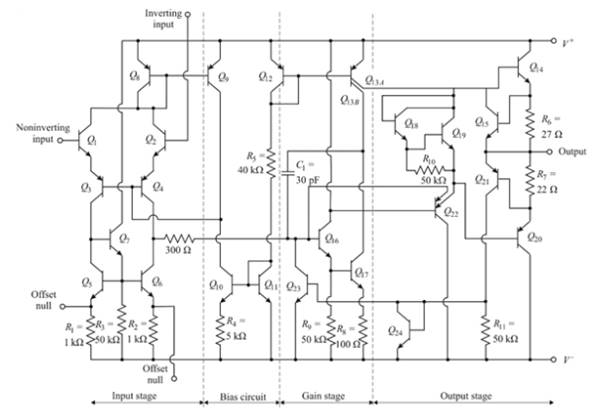
Calculation:
The reference current is.
Current
The bias currents in the input stage are,
The voltage at the collector of
The collector current in
Now, current
Assuming
The current in
The input resistance to the gain stage is found as
Therefore, the emitter resistor
Also
Consequently, the resistor value
Now the resistance of the active load is determined as
And
Then
Now the resistance
The small signal differential voltage is
The effective resistance of the active load is the resistance looking into the collector of
The small signal voltage gain is
The overall gain is
Want to see more full solutions like this?
Chapter 13 Solutions
Microelectronics: Circuit Analysis and Design


- NOTE: FOR ALL CIRCUITS SHOWN IN THIS QUIZ ASSUME THAT: β= 100 (for all transistors) ; Early voltage equal to infinity. 3. - For the circuit shown in figure C, determine the value of the gainAv = vo/vs Note: It is known that Vcc = 20varrow_forwardDesign a common-source amplifier such that gain is high and drain current is 11.33 amp. State the tech parameters and assumptions made.arrow_forwardDetermine Vceq of the given transistor configuration using the given collector voltage 15, collector resistance 2,072, base resistance 360,495, and current gain 87.arrow_forward
- 1: Determine the value of small-signal parameter gm of Q1 for the circuit shown below.arrow_forwardA base voltage of four volts is applied to an NPN bipolar junction transistor. A twenty kilo ohm resistor is linked to the base, while a hundred kilo ohm resistor is connected to the collector. The Collector is powered by a six volt supply voltage. Assume the transistor is in active mode, with a fifty common Emitter current gain(β).(i) Utilize the dc equivalent model of the transistor to draw the circuit design.(ii) Calculate the Collector current (IC) and the Base current (IB) .ii) Locate/determine the result (VCE).arrow_forwardDefine the common-mode rejection ratio of a differential amplifier.arrow_forward
- Subject : Electronics Engineering Draw the PNP transistor circuit in CB configuration. Sketch the output characteristics. Indicate active, saturation and cut off regions. Briefly explain the nature of these curves.arrow_forwardIn the circuit given in the figure, Vcc = 15V, R1 = R2 = 10k ohm, RE = 1k ohm, RL = 0.5k ohm and transistor parameters are given as VBE = 0.7V, beta (dc) = beta (0) = 100. According to this;a) Calculate the values of DC bias currents and voltages (I (BQ), I (CQ), V (CEQ)).b) Using the hybrid model of the transistor, draw the small signal equivalent circuit of the circuit.c) Derive the input impedance expression of the circuit and calculate its value.d) Derive the voltage gain expressions A (vi) and A (VG) and calculate its value.e) Derive the current gain expression A (i) = I (0) / I (i) and calculate its value. I sent you question's image. Thank you..arrow_forwardList and discuss the method to improve output signal-to-noise ratio (SNR) in amplifier configurationarrow_forward
- Topic: Field Effect Transistor Given the FET Amplifier circuit. Answer the question asked in each letter. a. Transconductance Gain (gm) b. Drain Resistor (RD) c. Input Impedance (Zi) d. Output Impedance (Zo) e. Voltage Gain (Av) f. What is the AC configuration of the amplifier?common source, common gate, common drain, or source bias?arrow_forwardDescribe the working principles of Bipolar Junction Transistor (BJT): Study of Single Stage Transistor Common Emitter Amplifierarrow_forwarda.) Consider a two-BJT configuration in Figure 1. You may assume that both transistors are the same with the same β, VBE,on = 0.7 V, and VCE,EOS = 0.3 V. Determine the minimum voltage VBE that will turn ON both Q1 and Q2. b.) Using the BJT small-signal model given in Figure 2, determine the AC current gain Ai = iout/iin for the circuit given in Figure 3. Assume ro >> rπ. You may assume that β is large.arrow_forward
 Introductory Circuit Analysis (13th Edition)Electrical EngineeringISBN:9780133923605Author:Robert L. BoylestadPublisher:PEARSON
 Delmar's Standard Textbook Of ElectricityElectrical EngineeringISBN:9781337900348Author:Stephen L. HermanPublisher:Cengage Learning
 Programmable Logic ControllersElectrical EngineeringISBN:9780073373843Author:Frank D. PetruzellaPublisher:McGraw-Hill Education
 Fundamentals of Electric CircuitsElectrical EngineeringISBN:9780078028229Author:Charles K Alexander, Matthew SadikuPublisher:McGraw-Hill Education
 Electric Circuits. (11th Edition)Electrical EngineeringISBN:9780134746968Author:James W. Nilsson, Susan RiedelPublisher:PEARSON
 Engineering ElectromagneticsElectrical EngineeringISBN:9780078028151Author:Hayt, William H. (william Hart), Jr, BUCK, John A.Publisher:Mcgraw-hill Education,