
(a)
The small signal differential-mode voltage gain.
(a)
Answer to Problem 13.5P
The overall small signal differential voltage gain
Explanation of Solution
Given:
The circuit diagram of the BJT op-amp is

Given that
The transistor parameters are,
And base-emitter turn-on voltage is
Calculation:
The differential mode voltage gain can be defined as
Where
From the figure the quiescent collector currents in
Hence,
The collector current for
Therefore, the collector current for
The transconductance can be calculated as
Therefore, the transconductance for
The resistance
Therefore, the resistance
The resistance
Therefore, the resistance
The resistance
Therefore, the resistance
The resistance
Therefore, the resistance
Substitute
Hence,
Substitute
Therefore, the differential mode voltage gain
The small signal voltage gain is

Now,
Therefore,
Where the resistance
Hence,
Equation(2) becomes
Therefore, the small signal voltage gain is
Now the overall small signal differential voltage gain is
Therefore, the overall small signal differential voltage gain
(b)
The differential-mode input resistance.
(b)
Answer to Problem 13.5P
The differential-mode input resistance is
Explanation of Solution
Given:
The circuit diagram of the BJT op-amp is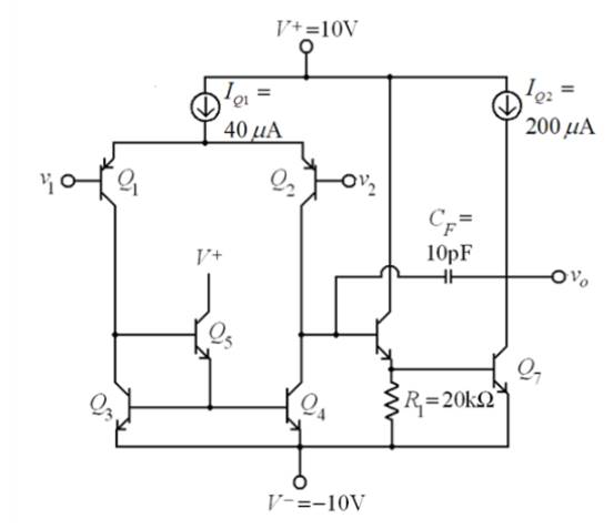
Given that
The transistor parameters are,
And base-emitter turn-on voltage is
Calculation:
The differential-mode input resistance is given as
Where
Hence,
Now, the differential-mode input resistance is
Therefore, the differential-mode input resistance is
(c)
Theunity-gain bandwidth.
(c)
Answer to Problem 13.5P
The gain bandwidth product is
Explanation of Solution
Given:
The circuit diagram of the BJT op-amp is

Given that
The transistor parameters are,
And base-emitter turn-on voltage is
Calculation:
The unity-gain bandwidth product is
Here, the dominant pole frequency is given as
Hence,
And
Hence,
Now the dominant pole frequency we obtain as
Therefore, the dominant pole frequency
The unity-gain bandwidth product is
Therefore, the gain bandwidth product is
Want to see more full solutions like this?
Chapter 13 Solutions
Microelectronics: Circuit Analysis and Design

- Output resistance??arrow_forwardThe transistors shown in Figure P12.43 operate in the active region and have β=100 and VBE=0.7 V. Determine IC and VCE for each transistor.arrow_forwardThe transistor having the characteristics shown in Figure P12.18 is operating with iC=8 mA and vCE = 12 V. Locate the point of operation on both the input and output characteristics.arrow_forward
- Describe the purpose and operating principle of UJT (unijunction transitor) and SCR amplifiersarrow_forwardConsider a 6 bit DIA converter with a resistance of 320 kΩ in LSB position. The converter is designed with weighted resistive network. The reference voltage is 10V. The output of the resistive network is connected to an OPAMP with feedback resistance of 5 kΩ. What is the output voltage for binary input of 111010?arrow_forwardDefine the common-mode rejection ratio of a differential amplifier.arrow_forward
- Define the term CMRR of a differential amplifier.arrow_forwardAnalyze the circuit of Figure P12.51 to determine IC and VCE.arrow_forwardSubject : Electronics Engineering Draw the PNP transistor circuit in CB configuration. Sketch the output characteristics. Indicate active, saturation and cut off regions. Briefly explain the nature of these curves.arrow_forward
- Each of the transistors shown in Figure P12.34 has β=100, |VCE|=0.2 V in saturation, and |VBE|=0.6 V in the active and saturation regions. For each transistor, determine the region of operation and the values of VCE, IB, IE and IC.arrow_forwardRefer to the differential amplifier circuit shown below . Determine the quiescent DC voltage at the collector terminal of each transistor assuming VBE of two transistor are negligible. What will be the quiescent DC values if VBE is taken to be 0.7 V.arrow_forwardImplement a buck converter with a PID controller and a voltage divider sensing unit using analog elements. Draw the schematic of your circuit?arrow_forward
 Introductory Circuit Analysis (13th Edition)Electrical EngineeringISBN:9780133923605Author:Robert L. BoylestadPublisher:PEARSON
 Delmar's Standard Textbook Of ElectricityElectrical EngineeringISBN:9781337900348Author:Stephen L. HermanPublisher:Cengage Learning
 Programmable Logic ControllersElectrical EngineeringISBN:9780073373843Author:Frank D. PetruzellaPublisher:McGraw-Hill Education
 Fundamentals of Electric CircuitsElectrical EngineeringISBN:9780078028229Author:Charles K Alexander, Matthew SadikuPublisher:McGraw-Hill Education
 Electric Circuits. (11th Edition)Electrical EngineeringISBN:9780134746968Author:James W. Nilsson, Susan RiedelPublisher:PEARSON
 Engineering ElectromagneticsElectrical EngineeringISBN:9780078028151Author:Hayt, William H. (william Hart), Jr, BUCK, John A.Publisher:Mcgraw-hill Education,