
Videos
In the circuit in Figure P14.38, the offset voltage of each op−amp is ±3 mV.
(a) Determine the possible range in output voltages
(b) Repeat part (a) for
(d) Design offset voltage compensation circuit(s) to adjust both
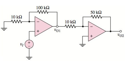
Figure P14.38
(a)
The possible range in output voltages
Answer to Problem 14.38P
The possible range in output voltages
Explanation of Solution
Given:
Given circuit:

Given offset voltage,
Calculation:
Now the input voltage is,
For the first op-amp which is a non-inverting amplifier, the gain is,
The possible range in the output voltage
For the second op-amp which is an inverting amplifier, the gain is,
Substitute
The possible range in the output voltage
Given
Above circuit can be represented as below

From equation
From equation (2) , the possible range in the output voltage
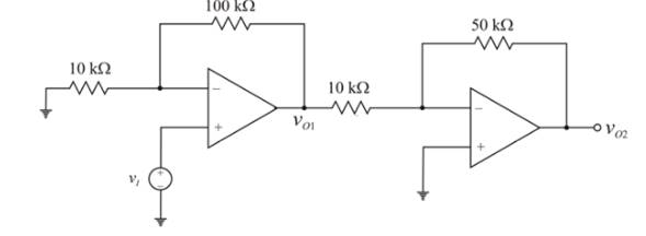
(b)
The possible range in output voltages
Answer to Problem 14.38P
The possible range in output voltages
Explanation of Solution
Given:
Given circuit:

Given offset voltage,
Calculation:
Now the input voltage is,
For the first op-amp which is a non-inverting amplifier, the gain is,
The possible range in the output voltage
For the second op-amp which is an inverting amplifier, the gain is,
Substitute
The possible range in the output voltage
Given
Above circuit can be represented as below

From equation
From equation (2), the possible range in the output voltage
(c)
The possible range in output voltages
Answer to Problem 14.38P
The possible range in output voltages
Explanation of Solution
Given:
Given circuit:

Given offset voltage,
The given value is
Calculation:
Now the input voltage is,
For the first op-amp which is a non-inverting amplifier, the gain is,
The possible range in the output voltage
For the second op-amp which is an inverting amplifier, the gain is,
Substitute
The possible range in the output voltage
Given
Above circuit can be represented as below

From equation
From equation (2) , the possible range in the output voltage
(d)
To design: The offset voltage compensation circuit(s) to adjust both
Answer to Problem 14.38P
The offset voltage compensation circuit is shown in Figure 1.
Explanation of Solution
Given:
Given circuit:
Given offset voltage,
Calculation:
The output voltages for the given input voltage
The adjusting compensation circuit for the range of output voltages as well as input voltage is shown below.
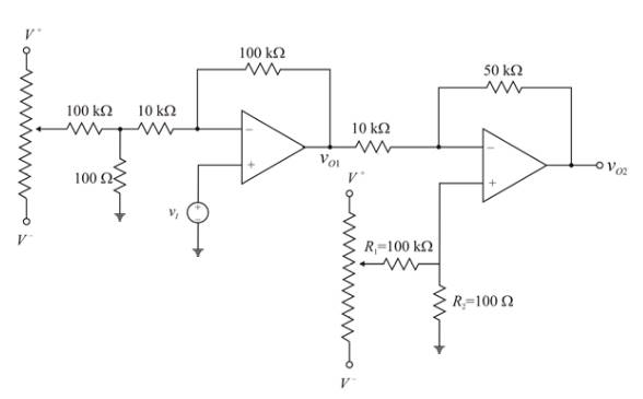
Figure 1
Want to see more full solutions like this?
Chapter 14 Solutions
Microelectronics: Circuit Analysis and Design


- Draw zener regulator circuit to obtain regulated DC voltage 6.8v . considering input DC voltage in the range from 10v to 30v . consider load resistance of 10kohmarrow_forwardRouth Hurwitz analysis of closed loop system with variable gain.arrow_forward3) Explain the construction, principle of operation, circuit and applications of Variable reluctance transducer with neat diagrams. 4) Describe the construction of LVDT and explain its principle of operation with the aid of diagram, list the advantages, disadvantages and applications of LVDT.arrow_forward
- Analyze the circuit of Figure P12.51 to determine IC and VCE.arrow_forwardDescribe this woofer it is Truvox 1225?arrow_forwardSuppose a power supply is energized by an AC source of 119 V RMS. The transformer step-down ratio is 8:1, it uses a full-wave bridge rectifier circuit with silicon diodes, and the filter is nothing but a single electrolytic capacitor. Calculate the unloaded DC output voltage for this supply (assume 0.7 volts drop across each diode). Also, write an equation solving for DC output voltage (Vout), given all these parameters.arrow_forward
- Find the following: DC gain, inductor current ripple and output voltage ripple: For DC-DC Buck converter: 1-Draw all circuits in all position 2-Sketch the transistor current waveform 3-Derive analytical expressions for the dc components of the capacitor voltages and inductor currents. 4-Derive analytical expressions for the peak ripple magnitudes of the input filter inductor current and capacitor voltage.arrow_forwardSketch the output voltage of the circuit shown in FigureP13.74 to scale versus time. Sometimes, an integrator circuit is used as a (approximate) pulse counter. Suppose that the output voltage is −10 V. How many input pulses have been applied (assuming that the pulses have an amplitude of 5 V and a duration of 2 ms, as shown in the figure)?arrow_forwardWhat is the output impedance of Common Emitter Collector Feedback preamplifier whose Collector Resistor is 2.7kohms, Feedback Resistor 180kohms?arrow_forward
- Problem: If the no-load output voltage of a regulator is 15.5 V and the full-load output is 14.9 V, what is the percent load regulation?arrow_forwardThe circuit diagram of step-up type DC-DC converter is given below. It is assumed that the output capacitor is large enough and the output voltage is constant. (Consider that there is no circuit losses.) Select an inductance value for the CCM operation state of the circuit. Assume that Output voltage (Vç) is regulated and prove that the circuit will always have to work at CCM operation state for maximum input voltage and minimum output current.arrow_forwardConsider the circuit of Figure 12.7 on page 605. Assume that VCC=20 V, VBB=0.3 V, RB=40 kΩ, and RC=2 kΩ. The input signal is a 0.2-V-peak 1-kHz sinusoid given by vin(t)=0.2 sin(2000πt). The common-emitter characteristics for the transistor are shown in Figure P12.18. Determine the maximum, minimum, and Q-point values for vCE. What is the approximate voltage gain for this circuit? Why is the gain so small in magnitude?arrow_forward
 Power System Analysis and Design (MindTap Course ...Electrical EngineeringISBN:9781305632134Author:J. Duncan Glover, Thomas Overbye, Mulukutla S. SarmaPublisher:Cengage Learning
 Electricity for Refrigeration, Heating, and Air C...Mechanical EngineeringISBN:9781337399128Author:Russell E. SmithPublisher:Cengage Learning