
a.
Range of output voltage for the given specifications.
a.
Answer to Problem 14.51P
The range of output voltage is,
Explanation of Solution
Given:
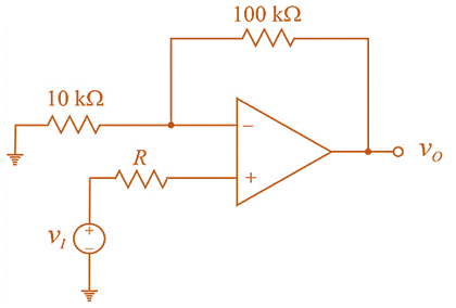
The given circuit is shown below.
Input offset voltage is
Average input bias current is
Offset bias current is
Calculation:
As,
And
Adding (1) and (2)
From (1)
For
For
Now, the modified circuit with offset voltage and bias current is shown below.
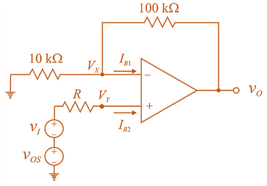
KCL at non-inverting terminal,
Now, for ideal op-amp
Now, KCL at inverting terminal,
Putting
Now,
For
For
For
0So, the range of output voltage is,
b.
Range of output voltage for the given specifications.
b.
Answer to Problem 14.51P
The range of output voltage is,
Explanation of Solution
Given:
The given circuit is shown below.

Input offset voltage is
Average input bias current is
Offset bias current is
Calculation:
From equation (4)
For
Putting the values,
For
For
So, the range of output voltage is,
c.
Range of output voltage.
c.
Answer to Problem 14.51P
The range of output voltage is,
Explanation of Solution
Given:
The given circuit is shown below.

Input offset voltage is
Average input bias current is
Offset bias current is
Calculation:
From equation (4)
For
Putting the values,
For
For
So, the range of output voltage is,
Want to see more full solutions like this?
Chapter 14 Solutions
Microelectronics: Circuit Analysis and Design

- In a DC-DC boost converter, the duty ratio is controlled to regulate the output voltage at 48 V. The input DC voltage is 24 V. The output power is 120 W. The switching frequency is 50 kHz. Assume ideal components and a very large output filter capacitor. The converter operates at the boundary between continuous and discontinuous conduction modes. The value of the boost inductor (in μH) isarrow_forwarda.Derive the excitation equations b. Determine transition and output equations c. Derive the transition/output table and Draw the state diagram.arrow_forwardIn Steady-State Operation o f Buck DC-DC Converter Explain how the switching frequency component is eliminated by the output filter network.arrow_forward
- Multiple Choice directions: Circle the letter of the answers that best answer the question. 13. When using microwave tubes as amplifiers, what is used as bandpass filters? a. Transistors b. Oscillator c. All of the above d. Power tubes 14. The microstrip lines used to achieve maximum power transfer are intended for a. Signal coupling b. Decoupling to prevent feedback c. Low-noise amplification d. Impedance matching and tuning 15. A diode that when reverse biased will momentarily and will abruptly turn off. a. Varactor diode b. IMPATT c. Step recovery diodes d. PIN diodes 16. A microwave transmission line used to minimize noise and crosstalks. a. Stripline b. Hard line cable c. Waveguide d. Microstrip 17. The major difference between a low frequency transistors and microwave types is/are. a. B & C b. Packaging c. Material d. Internal geometry 18. Which of the following band belongs to the millimeter waves a. C b. Ku c. U d. L 19. Overcrowding in the frequency spectrum is prevalent…arrow_forwardHow to analyze the circuit ? *Need excitation equation * Need transition equation *State transition table *Output equation * State diagramarrow_forwardQues 5: What is the Barkhausen criterion for feedback oscillator? Why do you use three RC sections in RCphase shift oscillators?arrow_forward
- determine voltaeg gainarrow_forwardConsider the circuit of Figure 12.7 on page 605. Assume that VCC=20 V, VBB=0.3 V, RB=40 kΩ, and RC=2 kΩ. The input signal is a 0.2-V-peak 1-kHz sinusoid given by vin(t)=0.2 sin(2000πt). The common-emitter characteristics for the transistor are shown in Figure P12.18. Determine the maximum, minimum, and Q-point values for vCE. What is the approximate voltage gain for this circuit? Why is the gain so small in magnitude?arrow_forwardProblem?) For a boost DC-DC Converter supplied by 100V, switching frequency 500HZ, on-period 600µsec, and load resistance 12. Compute the following: 1) DC output voltage, 2) DC output current, 3) Input DC current, 4) DC inductor current, and 5) The required input inductance and output filter capacitance so that reduce the input ripple current to 20% of the average input current and output ripple voltage to 10% of output average voltage.arrow_forward
- of a Flyback converter with Circuit parameters given below.Circuit Parameters;Input Voltage Vs= 48 VN1/N2=3Lm=500 μHR=5ΩC=200 μFSwitching frequency f=40 kHzOutput Voltage Vo=10 Va) Duty Cycleb) In terms of magnetization inductor (Lm); mean, maximum andtheir minimum values;c) Find the output voltage fluctuation. (All components are ideal.assume.)arrow_forwardsubject: Communication Fundamentals Modulation and Demodulationarrow_forward45) We have buck converter, the maximum current of the inductor is Imax, the minimum inductor currentIs Imin. We now know the period of the switching signal is T=20 µs, the duty cycle D is 0.5, the load resistance R is 2 ohms, the input voltage is 30V, and the inductance L is 100 µH; What is Imax andIs Imin?arrow_forward
 Electricity for Refrigeration, Heating, and Air C...Mechanical EngineeringISBN:9781337399128Author:Russell E. SmithPublisher:Cengage Learning