Concept explainers
Videos
(a) Design a two-stage op amp filter circuit with a bandwidth of 1000 rad/s, a low-frequency cutoff of 100 rad/s, and a voltage gain of 20 dB. (b) Verify your design with an appropriate LTspice simulation.
(a)
Design a two-stage op amp filter circuit with a bandwidth of
Explanation of Solution
Given data:
The value of the bandwidth
The value of the lower cutoff frequency
The value of the voltage gain
Formula used:
Write the expression to calculate the impedance of the passive elements resistor and capacitor.
Here,
Calculation:
The two-stage op amp filter circuit can be obtained in a band-pass filter by cascading the low pass filter and high pass filter.
In order to design the band-pass filter of gain
In two-stage op amp filter, the low pass op amp filter is the first stage and the output of first stage filter is given as an input of the second stage high-pass op amp filter.
Low-pass filter design:
For low-pass filter, the voltage gain
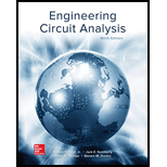
The active low-pass op amp filter is drawn as Figure 1.
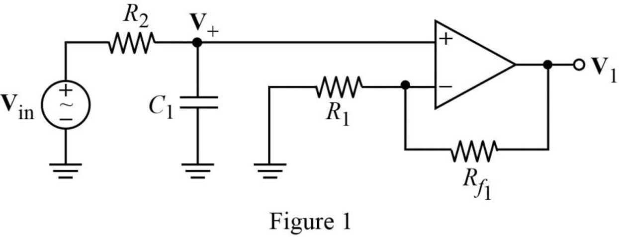
The s-domain circuit of the Figure 1 is drawn as Figure 2 using the equations (1) and (2).
Write the general expression to calculate the transfer function of the circuit in Figure 2.
Here,
Use nodal analysis on node
Rearrange the above equation to find
Use nodal analysis on node
Rearrange the above equation to find
It is known that for an ideal operational amplifier,
Substitute
Rearrange the above equation to find
Substitute
Therefore, the equation (4) is the transfer function of the active low-pass filter that is the product of the transfer function of general low-pass filter and the gain of the non-inverting amplifier.
From equation (4), the gain of non-inverting amplifier is,
Write the general expression to calculate the voltage gain in dB.
Substitute
Rearrange the above equation to find
Assume the resistor,
Substitute
n (5).
Rearrange the above equation to find
Write the expression to calculate the corner frequency of the filter circuit shown in Figure 1.
Assume the capacitor,
Write the expression to calculate the bandwidth of the filter.
It is known that the corner frequency
Substitute
Rearrange the above equation to find
Substitute
Rearrange the above equation to find
For first stage low-pass filter,
High-pass filter design:
For high-pass filter, the voltage gain
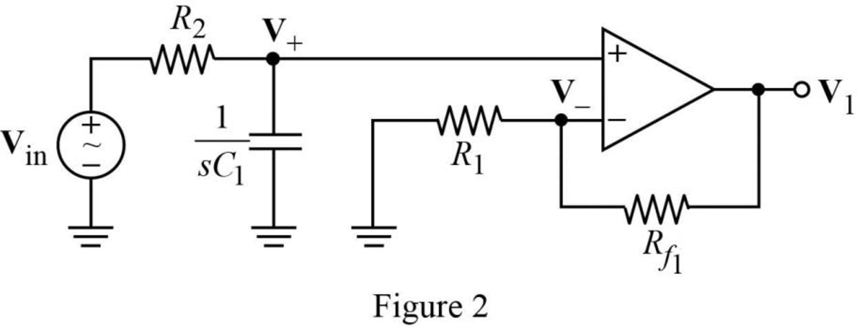
The active high-pass op amp filter is drawn as Figure 3.
The s-domain circuit of the Figure 3 is drawn as Figure 4 using the equations (1) and (2).
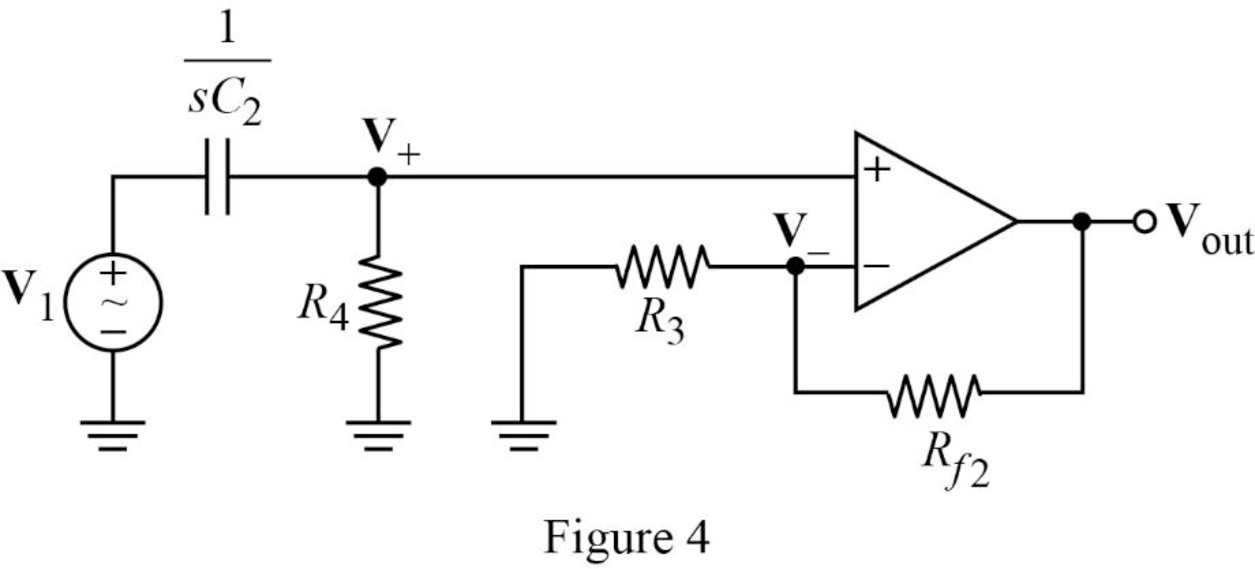
Write the general expression to calculate the transfer function of the circuit in Figure 4.
Here,
Use nodal analysis on node
Rearrange the above equation to find
Use nodal analysis on node
Rearrange the above equation to find
It is known that for an ideal operational amplifier,
Substitute
Rearrange the above equation to find
Substitute
Therefore, the equation (8) is the transfer function of the active high-pass filter that is the product of the transfer function of general high-pass filter and the gain of the non-inverting amplifier.
From equation (8), the gain of non-inverting amplifier is,
Write the general expression to calculate the voltage gain in dB.
Substitute
Rearrange the above equation to find
Assume the resistor,
Substitute
Rearrange the above equation to find
Write the expression to calculate the corner frequency of the filter circuit shown in Figure 4.
Assume the capacitor,
It is known that the corner frequency
Given that,
Substitute
Rearrange the above equation to find
Simplify the above equation to find
For second stage high-pass filter,
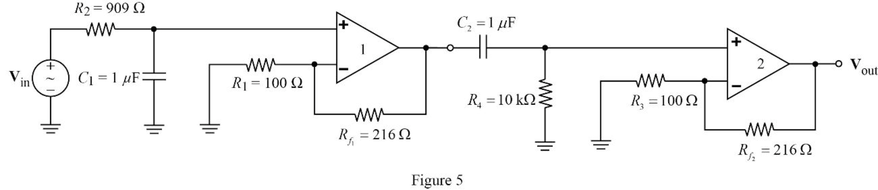
The two-stage op amp band-pass filter circuit is drawn as Figure 5.
Conclusion:
Thus, the two-stage op amp filter circuit with a bandwidth of
(b)
Verify the two-stage op amp filter circuit design with an appropriate LTspice simulation.
Explanation of Solution
Calculation:
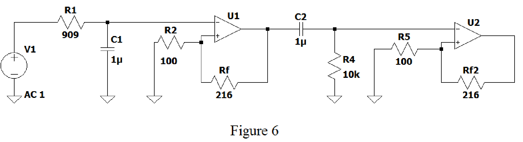
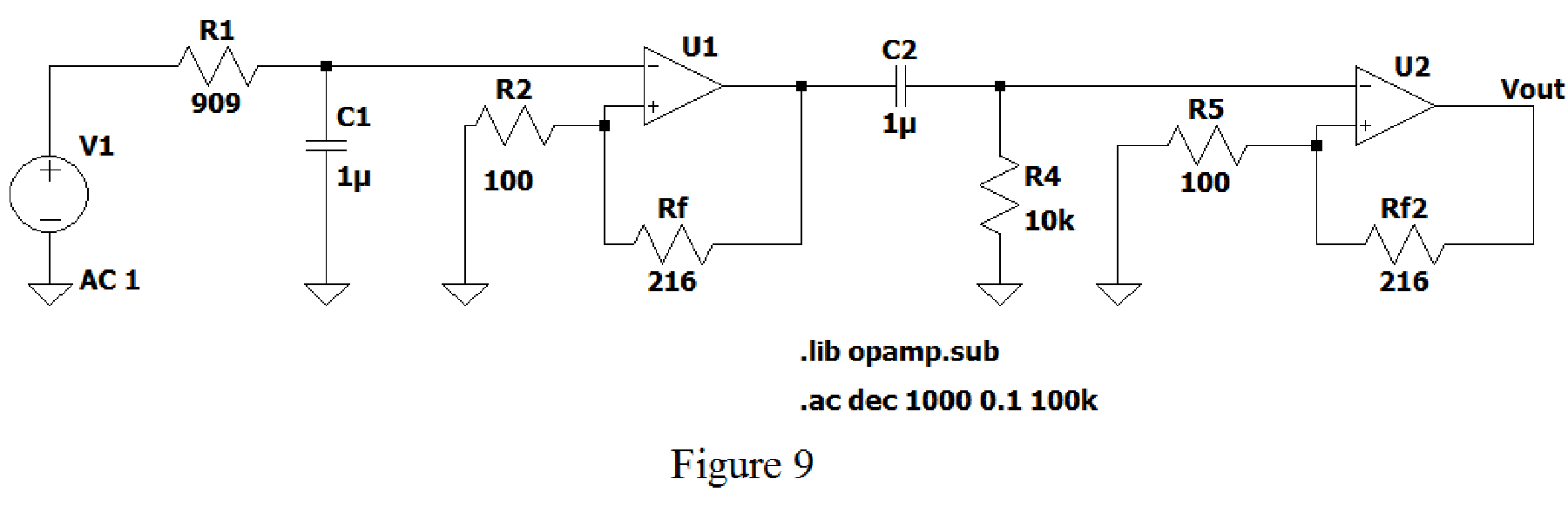
Create the new schematic in LTspice and draw the circuit in Figure 5 as shown in Figure 6 by entering the corresponding values of resistors and capacitors.
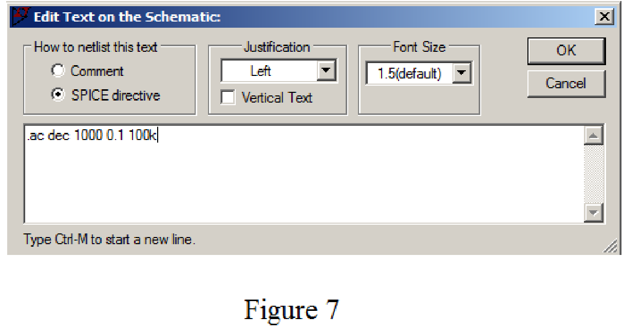
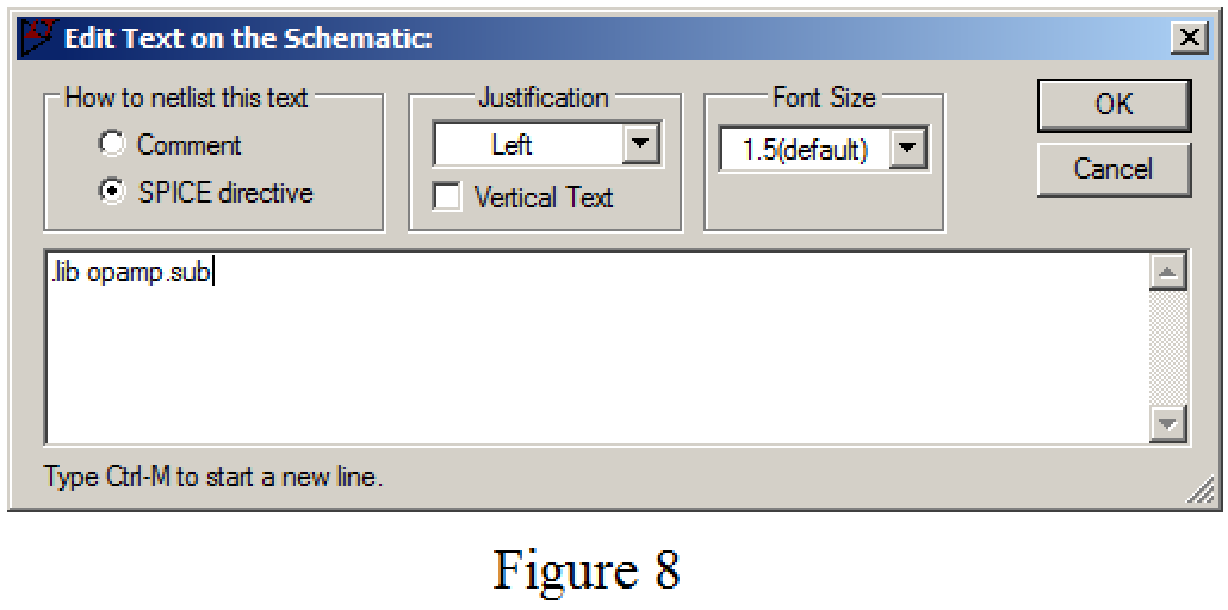
Using SPICE Directive in Edit menu, mention the command .ac dec 1000 0.1 100k and .lib opamp.sub as shown in Figure 7 and Figure 8.
Use Label Net option and enter the Vout. After adding all the commands mentioned above, the circuit is shown as in Figure 9.
Now run the simulation and place the probe at resistor
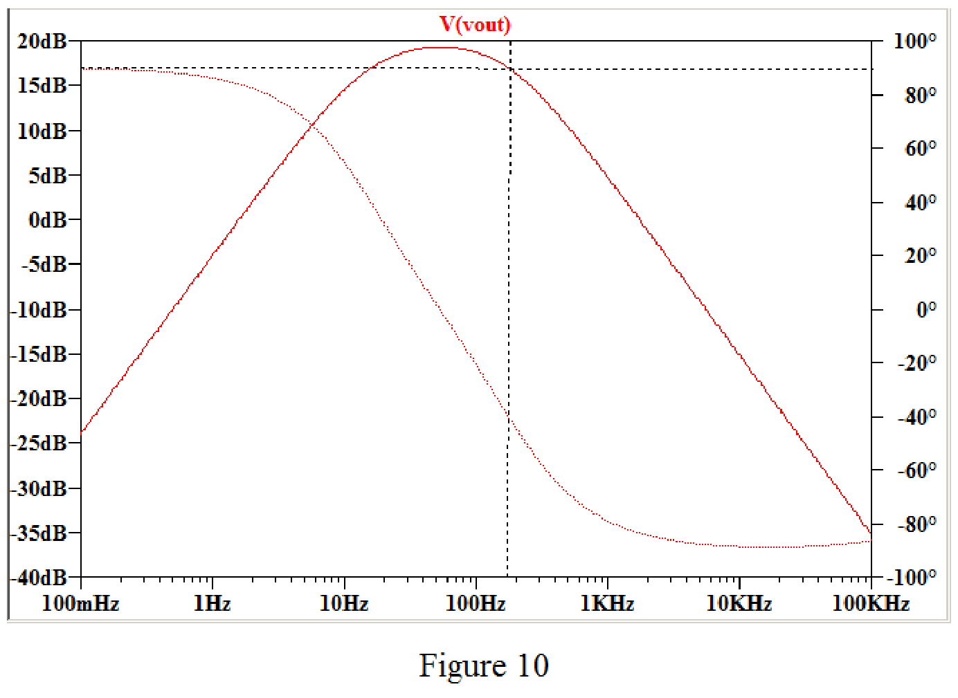
Refer to Figure 10 the thick red line indicates magnitude response, the dotted red line indicates phase response, and the black dotted line represents the corner frequency of the magnitude response.
Conclusion:
Thus, the design of the two-stage op amp filter is verified by using the LTspice simulation.
Want to see more full solutions like this?
Chapter 15 Solutions
Loose Leaf for Engineering Circuit Analysis Format: Loose-leaf
Additional Engineering Textbook Solutions
Basic Engineering Circuit Analysis
Principles and Applications of Electrical Engineering
Electric Circuits. (11th Edition)
Engineering Electromagnetics
Electronics Fundamentals: Circuits, Devices & Applications
Electric Motors and Control Systems


- The voltage transfer function of the prototype bandpass filtershown isH(s)=(1Q)ss2+(1Q)s+1. Show that if the circuit is scaled in both magnitude and frequency, thescaled transfer function isH′(s)=(1Q)(skf)(skf)2+(1Q)(skf)+1.arrow_forwardDESIGNPROBLEM_PSPICEMULTISIM Use a 500 nF capacitor to design a bandreject filter, as shown . The filter has a center frequency of 4 kHz and a quality factor of 5. 1. a) Specify the numerical values of R and L. 2. b) Calculate the upper and lower corner, or cutoff, frequencies in kilohertz. 3. c) Calculate the filter bandwidth in kilohertz.arrow_forwardDESIGNPROBLEM_1. Using the circuit, design a low-pass filter with apassband gain of 5 dB and a cutoff frequency of 10 kHz. Assume a50 nF capacitor is available.2. Draw the circuit diagram and label all components.arrow_forward
- Design a unity-gain parallel bandreject filter with a centerfrequency of 250 rad/s and a bandwidth of 2000 rad/s. Use 1 μFcapacitors, and specify all resistor values.arrow_forwardOn the circuit below, assume all initial conditions are 0 and that R = 1kΩ, L = 1mH, and C = 1uF. 1. What is the pass band gain?2. Sketch by hand the bode plots of the system. Clearly explain your reasoning.arrow_forwardFind the gain of the following circuit and the lower and upper cutoff frequencies. (RS = 1 kΩ, R1 = 40 kΩ, R2 = 10kΩ, RC = 20 kΩ, RE = 30 kΩ, RL = 2.2 kΩ, CS = 10 µF, CC = 1 µF, CE = 20 µF, Cbe = 20 pF, Cbc = 30 pF,VT = 26mV, β = 100, ro = infinityarrow_forward
- In an LR−C network, the capacitance is 10.61 nF, the bandwidth is 500 Hz and the resonant frequency is 150 kHz. Determine for the circuit the Q-factor, the dynamic resistance, and the magnitude of the impedance when the supply frequency is 0.4% greater than the tuned frequency.arrow_forwardDESIGNPROBLEM_Using a 100 nF capacitor, design a highpass passive filter with a cutoff frequency of 300 Hz. 1. a) Specify the value of R in kilohms. 2. b) A 47 kΩ resistor is connected across the output terminals of the filter. What is the cutoff frequency, in hertz, of the loaded filter?arrow_forwardQ2/Design a filter that pass all frequencies between 30khz and 60khz ? *arrow_forward
- Using cascading, design an active low pass filter with the following specifications:Amax = 1 dBAmin = 30 dBfp = 20 kHzfs = 40 kHzThe filter order N should be as small as possible. Choose only from the filter that you have studied.Draw your circuit and show all calculations for the component values, with justifications explained (where applicable).arrow_forwardBe able to use design equations to calculate componentvalues for prototype narrowband bandpass, and bandreject filters Design an active bandpass filter with Q=8, K=5, and ωo=1000 rad/s. Use 1 μF capacitors, and specify the values of all resistors.arrow_forwardWrite a program to design a bandpass analog Butterworth that pass the frequency 20 rad/sec for the signal x(t) = sin(20t) + sin(40t) . then 1- Plot the filtered signal (time domain and spectrum). 2- Plot the frequency response of the filter. 3- Verify your resultarrow_forward
 Introductory Circuit Analysis (13th Edition)Electrical EngineeringISBN:9780133923605Author:Robert L. BoylestadPublisher:PEARSON
 Delmar's Standard Textbook Of ElectricityElectrical EngineeringISBN:9781337900348Author:Stephen L. HermanPublisher:Cengage Learning
 Programmable Logic ControllersElectrical EngineeringISBN:9780073373843Author:Frank D. PetruzellaPublisher:McGraw-Hill Education
 Fundamentals of Electric CircuitsElectrical EngineeringISBN:9780078028229Author:Charles K Alexander, Matthew SadikuPublisher:McGraw-Hill Education
 Electric Circuits. (11th Edition)Electrical EngineeringISBN:9780134746968Author:James W. Nilsson, Susan RiedelPublisher:PEARSON
 Engineering ElectromagneticsElectrical EngineeringISBN:9780078028151Author:Hayt, William H. (william Hart), Jr, BUCK, John A.Publisher:Mcgraw-hill Education,