
Videos
(a)
The transition point and value of
(a)
Answer to Problem 16.2P
The transition point is,
The value of
Explanation of Solution
Given:
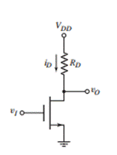
The given circuit is shown below.
The parameters are:
Calculation:
For the transition point, the equation for finding the input voltage is,
Substituting the values,
Solving the above quadratic equation,
Ignoring the negative term, the input voltage of transition point is
Now, the output voltage at the transition point is
It is given that input voltage is
Substituting the values in the above equation,
Solving the above quadratic equation,
Since, the output voltage cannot be greater than
The output voltage will be
Conclusion:
Therefore, the transition points are
Also, the value of
(b)
The transition point and value of
(b)
Answer to Problem 16.2P
The transition point is,
The value of
Explanation of Solution
Given:
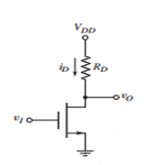
The given circuit is shown below.
The parameters are:
Calculation:
For the transition point, the equation for finding the input voltage is,
Substituting the values,
Solving the above quadratic equation,
Ignoring the negative term, the input voltage of transition point is
Now, the output voltage at the transition point is
It is given that input voltage is
Substituting the values in the above equation,
Solving the above quadratic equation,
Since, the output voltage cannot be greater than
The output voltage will be
Conclusion:
Therefore, the transition points are
Also, the value of
(c)
The transition point and value of
(c)
Answer to Problem 16.2P
The transition point is,
The value of
Explanation of Solution
Given:
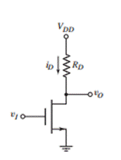
The given circuit is shown below.
The parameters are:
Calculation:
For the transition point, the equation for finding the input voltage is,
Substituting the values,
Solving the above quadratic equation,
Ignoring the negative term, the input voltage of transition point is
Now, the output voltage at the transition point is
It is given that input voltage is
Substituting the values in the above equation,
Solving the above quadratic equation,
Since, the output voltage cannot be greater than
The output voltage will be
Conclusion:
Therefore, the transition points are
Also, the value of
Want to see more full solutions like this?
Chapter 16 Solutions
Microelectronics: Circuit Analysis and Design


- 16.44 A ring-of-nine oscillator is found to operate at 20 MHz. Find the propagation delay of the inverter.arrow_forwardIf,for a single phase half bridge inverter the amplitude of output voltage is Vs and the output power is P then their corresponding values for a single phase full-bridge inverter are a. 2Vs,2P b. 2Vs,4P c. 2Vs,P d. Vs,Parrow_forwardAn industry has 4 shareholders(W,X,Y,Z). 35 percent, 30 percent ,25 percent and 10 percent are the % of shares held by the shareholders, respectively.60 percent or above of the stack of full support is required for any main decision to be taken in the industry. Hint: Voting power of shareholders = Shares held by them i.Using only NAND gates illustrate how the circuit could be implemented. ii.Considering the voting in the industry, there should be a designation of a combinational logic circuit.(Note the design should relate to the voting in the industry)arrow_forward
- Consider two microprocessors having 8-bit and 16-bit wide external data buses, respectfully. The two processors are identical otherwise and their bus cycles are the same speed. Suppose all instructions and operands are two Bytes. By what factor do the maximum data transfer rates vary? Suppose all instructions and operands are one Byte. By what factor do the maximum data transfer rates vary? Discuss your answers.arrow_forwardpower electronics 1- For half-bridge inverter circuit loaded with RLC, input voltage (Vs/2) = 115 V, output frequency is given as 50Hz. Since R=4 ohm , L = 35 mH and C = 155 micro F, which option gives the correct expression of the output voltage up to the 5th harmonic.arrow_forward20.a. More spares should be purchased for equipment with a smallA. receiver sensitivity threshold.B. mean time between failures.C. channel spacing.D. optical return loss.20.b. How many OC signals are combined into a 40 Gbps SONET network?A. 192B. 256C. 768D. 516,096arrow_forward
- Suppose a ring oscillator is built from N inverters connected in a loop. Each inverter has a minimum delay of tcd and a maximum delay of tcd. If N is odd, determine the range of frequencies at which the oscillator might operate.arrow_forwardDraw the schematic of the designed decoder (using 2-input & 3-input NAND gates, and one inverter):arrow_forwardDESIGN A 16X1 MUX IN ORDER TO SATISFY THE FUNCTION F(A,B,C,D)=SUM(0,3,6,7,8,10,13,15) USING: B) 4X1 MULTIPLEXERS using 74151arrow_forward
- Assume that our MAR contains 20 bits, enabling us to access up to 220 memory cells, which is 1 MB, but our computer has 4 MB of memory. Explain how it might be possible to address all 4 MB memory cells using a MAR that contains only 20 bits. Assume that our MDR register is 16 bits wide while our machine language instructions are 32 bits wide. How might the fetch phase of the Von Neumann cycle have to be changed from what was described in the text? Assume that a 1 gigaflop machine is connected to a printer that can print 780 characters per second. In the time it takes to print 1 page (65 lines of 60 characters per line), how many floating-point operations can the machine perform? Assume that we have an arithmetic/logic unit that can carry out 20 distinct operations. Describe exactly what kind of multiplexer circuit would be needed to select exactly one of those 20 operations.arrow_forwardDesign transistor level circuits for a 4-bit even parity generator using (i) CCMOS logic (ii) pseudo-nmos logic (iii) pass transistor logic, (iv) transmission gate logic.arrow_forwardImplement F(A,B,C)= m2+m5+m6+m7, using the smallest possible multiplexer and inverters as needed.arrow_forward
 Introductory Circuit Analysis (13th Edition)Electrical EngineeringISBN:9780133923605Author:Robert L. BoylestadPublisher:PEARSON
 Delmar's Standard Textbook Of ElectricityElectrical EngineeringISBN:9781337900348Author:Stephen L. HermanPublisher:Cengage Learning
 Programmable Logic ControllersElectrical EngineeringISBN:9780073373843Author:Frank D. PetruzellaPublisher:McGraw-Hill Education
 Fundamentals of Electric CircuitsElectrical EngineeringISBN:9780078028229Author:Charles K Alexander, Matthew SadikuPublisher:McGraw-Hill Education
 Electric Circuits. (11th Edition)Electrical EngineeringISBN:9780134746968Author:James W. Nilsson, Susan RiedelPublisher:PEARSON
 Engineering ElectromagneticsElectrical EngineeringISBN:9780078028151Author:Hayt, William H. (william Hart), Jr, BUCK, John A.Publisher:Mcgraw-hill Education,