
Concept explainers
Videos
(a)
The value of the input switching voltage and the input voltage for the given
(a)
Answer to Problem 16.33P
The value of the input switching voltage is
Explanation of Solution
Calculation:
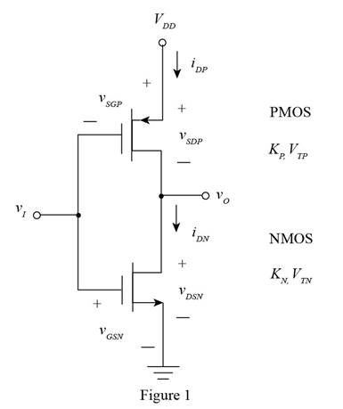
The given diagram is shown in Figure 1
The expression to determine the trans-conductance parameter for NMOS is given by,
Substitute
The expression to determine the trans-conductance parameter for PMOS is given by,
Substitute
The expression to determine the transition points
Substitute
The expression to determine the value of the input voltage is given by,
Substitute
The expression to determine the value of the input voltage when the output voltage is more than
Substitute
Conclusion:
Therefore, the value of the input switching voltage is
(b)
The value of the input switching voltage and the input voltage for the given
(b)
Answer to Problem 16.33P
The value of the input switching voltage is
Explanation of Solution
Calculation:
The expression to determine the trans-conductance parameter for NMOS is given by,
Substitute
The expression to determine the trans-conductance parameter for PMOS is given by,
Substitute
The expression to determine the transition points
Substitute
The expression to determine the value of the input voltage is given by,
Substitute
The expression to determine the value of the input voltage when the output voltage is more than
Substitute
Conclusion:
Therefore, the value of the input switching voltage is
Want to see more full solutions like this?
Chapter 16 Solutions
Microelectronics: Circuit Analysis and Design


- A CMOS inverter has (W/L)N =2/1,(W/L)P =5/1 for VDD = 2.0 V, VTN =0.45 V, and VTP = −0.55 V. for VDD = 2.0 V, VTN = 0.55 V,and VTP = −0.45 V.What is the peak current in the logicgate and at what input voltage does it occur?arrow_forward1. A square-wave inverter has an R-L load with R=15 Ω and L=10 mH. The inverter output frequency is400 Hz (fundamental frequency).(a) Determine the values of the required to establish a load current which has a fundamentalfrequency component of 10 A rms with α = 0.(b) For a controlled full-bridge inverter, the dc source is 125 V and the switching frequency is60 Hz. Determine the value of α to produce an output with amplitude of 100 V at the fundamentalfrequency.arrow_forwardWire delay I. Calculate the delay of a 10 mm wire in 28 nm technology that is divided into 20 0.5 mm segments with a 20× minimum-size inverter driving each segment.arrow_forward
- What are the noise margins of a minimum size CMOS inverter in which both W/L ratios are 2/1 and VDD = 2.5 V and VTN = −VTP = 0.6 V?arrow_forwardWhat is the power-delay product for a symmetrical CMOSinverter with (W/L)N = 2/1, (W/L)P = 5/1,VDD = 2.5 V, and C = 0.3 pF? (b) Repeat forVDD = 2.0 V. (c) Repeat for VDD = 1.8 V.? How much power does the inverter dissipate if it is switching at a frequency of 100 MHz?arrow_forwardPlease can you explain why a 13-bit analogue-to digital-convertor (ADC) is often used in pulse code modulation (PCM) when only 8-bits are transmitted. Then, why following compression in PCM, how and why is an inverter used?arrow_forward
- Design a reference inverter to achieve a delay of 250 ps when driving a 0.2-pF load using a 3.3-V power supply. Assume that the threshold voltages of the CMOS technology are VTN = −VTP = 0.75 V.what W/L ratios are required to actually achieve an average propagation delay of 250 ps?arrow_forwardGiven Vdd=3.3V, Kn=100uA/V2 , Kp=20uA/V2,Vtn = 0.6V, and Vtp = -0.6V. Determine the Voltage Transfer Characteristics points indicated by the pseudo-NMOS inverter circuit.arrow_forwardImplement F(A,B,C)= m2+m5+m6+m7, using the smallest possible multiplexer and inverters as needed.arrow_forward
- Describe the C-V characteristics of a MOS capacitor and explain the physics behind them. 2. Draw the IV curve of a MOSFET for different gate voltages. Explain the characteristics of the curve and dependence on the gate voltage. 3. Explain the structure and operation principle of a CMOS inverter. What are its benefits? 4. Compare SRAM, DRAM and Flash memoriesarrow_forwardDesign an asymmetrical inverter to meet the delay specification a symmetrical CMOS reference inverter to provide a propagation delay of 400 ps fora load capacitance of 200 fF. Use VDD =2.5 V, VTN =0.60 V, and VTP =−0.60 V.with (W/L)P = (W/L)N .arrow_forwardSuppose a ring oscillator is built from N inverters connected in a loop. Each inverter has a minimum delay of tcd and a maximum delay of tcd. If N is odd, determine the range of frequencies at which the oscillator might operate.arrow_forward
 Introductory Circuit Analysis (13th Edition)Electrical EngineeringISBN:9780133923605Author:Robert L. BoylestadPublisher:PEARSON
 Delmar's Standard Textbook Of ElectricityElectrical EngineeringISBN:9781337900348Author:Stephen L. HermanPublisher:Cengage Learning
 Programmable Logic ControllersElectrical EngineeringISBN:9780073373843Author:Frank D. PetruzellaPublisher:McGraw-Hill Education
 Fundamentals of Electric CircuitsElectrical EngineeringISBN:9780078028229Author:Charles K Alexander, Matthew SadikuPublisher:McGraw-Hill Education
 Electric Circuits. (11th Edition)Electrical EngineeringISBN:9780134746968Author:James W. Nilsson, Susan RiedelPublisher:PEARSON
 Engineering ElectromagneticsElectrical EngineeringISBN:9780078028151Author:Hayt, William H. (william Hart), Jr, BUCK, John A.Publisher:Mcgraw-hill Education,