
Videos
(a)
The output voltage
(a)
Answer to Problem 16.3EP
The output voltage
Explanation of Solution
Given:
Power supply voltage,
Intrinsic trans conductance parameter,
Device parameter for driver transistor,
Device parameter for load transistor,
Aspect ratio of driver transistor,
Aspect ratio of load transistor,
When input voltage,
Calculation:
Given depletion-load NMOS inverter:
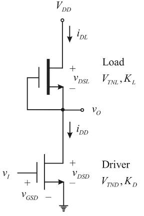
For the NMOS inverter with Depletion load, the output voltage equation is given by
The parameters
Now substituting all the values in the above voltage equation,
On comparing the above equation with quadratic equation
The output voltage cannot be greater than
Conclusion:
Therefore, the output voltage
(b)
The maximum current and maximum power dissipation in the inverter.
(b)
Answer to Problem 16.3EP
The maximum current and maximum power dissipation in the inverter are
Explanation of Solution
Given:
Power supply voltage,
Intrinsic trans conductance parameter,
Device parameter for driver transistor,
Device parameter for load transistor,
Aspect ratio of driver transistor,
Aspect ratio of load transistor,
Calculation:
Maximum current is
Maximum Power dissipated in the inverter is
Conclusion:
Therefore, maximum current and maximum power dissipation in the inverter are
(c)
The transition points for the driver and load transistors.
(c)
Answer to Problem 16.3EP
The transition points for the driver and load transistors are
Explanation of Solution
Given:
Power supply voltage,
Intrinsic trans conductance parameter,
Device parameter for driver transistor,
Device parameter for load transistor,
Aspect ratio of driver transistor,
Aspect ratio of load transistor,
When input voltage,
Calculation:
Transition points for the driver transistor
Output transition point is
Transition points for the load transistor
Output transistor point is
Conclusion:
The transition points for the driver and load transistors are
Want to see more full solutions like this?
Chapter 16 Solutions
Microelectronics: Circuit Analysis and Design


- If a 3 phase inverter is feeding an appliance that is rated as 207v AC, 60Hz, 100kVA, compute the minimum DC input voltage, that must be feed to the inverter. Assume the Modulation Index Ma to 1. ...arrow_forward1. Draw the transistor level Diagram for the expression Y = (A+B) C+CD using CMOS technology. Also sketch the stick diagram. 2. Describe the read and write operation of a 6T SRAM cell with necessary figures.arrow_forwardGiven Vdd=3.3V, Kn=100uA/V2 , Kp=20uA/V2,Vtn = 0.6V, and Vtp = -0.6V. Determine the Voltage Transfer Characteristics points indicated by the pseudo-NMOS inverter circuit.arrow_forward
- Design an asymmetrical inverter to meet the delay of 250 ps for a load capacitance of 120 fF. Use VDD =1.5V, VTN =0.50 V, and VTP =−0.50 V. with (W/L)P = (W/L)N .arrow_forwardSuppose a ring oscillator is built from N inverters connected in a loop. Each inverter has a minimum delay of tcd and a maximum delay of tpd. If N is odd, determine the range of frequencies at which the oscillator might operate.arrow_forward1. Four 1KB EPROMs are used to make a 4KB memory. How many address lines are needed for each EPROM? Design an address decoder circuit.arrow_forward
- Subject name: Microcomputer application principle Question: Four 1KB EPROMs are used to make a 4KB memory. How many address lines are needed for each EPROM? Design an address decoder circuit.arrow_forwardAssume that our MAR contains 20 bits, enabling us to access up to 220 memory cells, which is 1 MB, but our computer has 4 MB of memory. Explain how it might be possible to address all 4 MB memory cells using a MAR that contains only 20 bits. Assume that our MDR register is 16 bits wide while our machine language instructions are 32 bits wide. How might the fetch phase of the Von Neumann cycle have to be changed from what was described in the text? Assume that a 1 gigaflop machine is connected to a printer that can print 780 characters per second. In the time it takes to print 1 page (65 lines of 60 characters per line), how many floating-point operations can the machine perform? Assume that we have an arithmetic/logic unit that can carry out 20 distinct operations. Describe exactly what kind of multiplexer circuit would be needed to select exactly one of those 20 operations.arrow_forward16.44 A ring-of-nine oscillator is found to operate at 20 MHz. Find the propagation delay of the inverter.arrow_forward
- Design an asymmetrical inverter to meet the delay specification a symmetrical CMOS reference inverter to provide a propagation delay of 400 ps fora load capacitance of 200 fF. Use VDD =2.5 V, VTN =0.60 V, and VTP =−0.60 V.with (W/L)P = (W/L)N .arrow_forwardAssume the following values for the inverter circuit parameters: Vs = 6v, VT = 0.9v RL = 5kΩ, k’nVOV = 0.25 Determine a (W/L) sizing for the MOSFET so that the inverter gate output for a logical 0 is able to switch OFF the MOSFET of another inverter.arrow_forwardWhat is the power-delay product for a symmetrical CMOSinverter with (W/L)N = 2/1, (W/L)P = 5/1,VDD = 2.5 V, and C = 0.3 pF? (b) Repeat forVDD = 2.0 V. (c) Repeat for VDD = 1.8 V.? How much power does the inverter dissipate if it is switching at a frequency of 100 MHz?arrow_forward
 Introductory Circuit Analysis (13th Edition)Electrical EngineeringISBN:9780133923605Author:Robert L. BoylestadPublisher:PEARSON
 Delmar's Standard Textbook Of ElectricityElectrical EngineeringISBN:9781337900348Author:Stephen L. HermanPublisher:Cengage Learning
 Programmable Logic ControllersElectrical EngineeringISBN:9780073373843Author:Frank D. PetruzellaPublisher:McGraw-Hill Education
 Fundamentals of Electric CircuitsElectrical EngineeringISBN:9780078028229Author:Charles K Alexander, Matthew SadikuPublisher:McGraw-Hill Education
 Electric Circuits. (11th Edition)Electrical EngineeringISBN:9780134746968Author:James W. Nilsson, Susan RiedelPublisher:PEARSON
 Engineering ElectromagneticsElectrical EngineeringISBN:9780078028151Author:Hayt, William H. (william Hart), Jr, BUCK, John A.Publisher:Mcgraw-hill Education,