
(a)
The value of the current and voltage
(a)
Answer to Problem 17.15P
The value of the current
Explanation of Solution
Calculation:
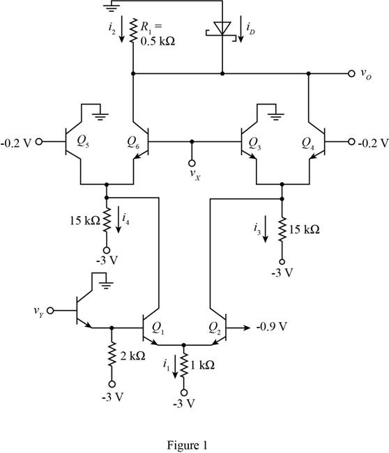
The given diagram is shown in Figure 1.
The expression for the current
Substitute
The expression to determine the value of the current
Substitute
The expression to determine the value of the current
Substitute
The expression for the value of the current
Substitute
The expression to determine the value of the current
Substitute
The output voltage is the voltage of the diode with opposite polarity and is given by,
Conclusion:
Therefore, the value of the current
(b)
The value of the current and voltage
(b)
Answer to Problem 17.15P
The value of the current
Explanation of Solution
Calculation:
The diode
The expression for the current
Substitute
The expression to determine the value of the current
Substitute
The expression to determine the value of the current
Substitute
The expression to determine the value of the current
Substitute
The expression to determine the value of the output voltage is given by,
Substitute
Conclusion:
Therefore, the value of the current
(c)
The value of the current and voltage
(c)
Answer to Problem 17.15P
The value of the current
Explanation of Solution
Calculation:
The transistor
The expression for the current
Substitute
The expression to determine the value of the current
Substitute
The expression to determine the value of the current
Substitute
The diode is in the cut off and the diode current is given by,
The expression to determine the value of the current
Substitute
The expression to determine the value of the output voltage is given by,
Substitute
Conclusion:
Therefore, the value of the current
(d)
The value of the current and voltage
(d)
Answer to Problem 17.15P
The value of the current
Explanation of Solution
Calculation:
The transistor
The expression for the current
Substitute
The expression to determine the value of the current
Substitute
The expression to determine the value of the current
Substitute
The expression for the value of the current
Substitute
The expression to determine the value of the current
Substitute
The output voltage is the voltage of the opposite polarity and is given by,
Conclusion:
Therefore, the value of the current
Want to see more full solutions like this?
Chapter 17 Solutions
Microelectronics: Circuit Analysis and Design

- For a PCM system with the following parameters, Parameters: (i) Maximum analog input frequency = 5 kHz; (ii) Maximum decoded voltage at the receiver = ±5.01 V; (iii) Minimum dynamic range = 54 dB. (Use 2 decimal places) a) What is the coding efficiency in % b) What is the resolution in V? c) Determine the maximum quantization error in V. d) Determine the minimum sampling rate in KHz e)Determine minimum number of bits use for the PCM code excluding sign bit.arrow_forward1. a. Create the gray code representation of the following binary numbers.i) 01011 ii) 10110 iii) 01101 iv) 11001 b. If a computer’s system clock is 2.7 GHz, calculate the period of the system clock. c. What is the minimum sampling rate needed in order to successfully capture frequencies up to 60MHz in an analog signal? d. Represent the number 1.00011011101 x 2-23in IEEE Standard 754 single precision floating point binary.arrow_forwardConstruct the circuit using RTL (resistor transistor logic) components for the function; F(A,B,C,D)=E(0,4,8,12,14).arrow_forward
- State the advantages and disadvantages of theDSB_LCarrow_forward10. both inputs of a NAND LATCH are low, then the S input goes HIGH . shortly thereafter, the R input goes HIGH, the state of the latch is? 11. how many stable states does a latch has?arrow_forwardEstimate the gate capacitance of PMOS transistor (? = 0.36?, ? =0.18?). Gate oxide thickness is 40Å . Relative permittivity of silicon dioxide is 3.9. Vacuumpermittivity ?0 = 8.854 ? 10−12F·?−1. Answer in fF , round off to 4 decimal places.arrow_forward
- An ADC has a uniform quantizer followed by a 7-bit binary encoder. The bit rate of the system is 50Mbps. What is the maximum frequency of the analog signal for which system operation is satisfactory?arrow_forward(a) What are the output currents in the circuit shown in P16.16 (a)if the area of transistor Q1 is changed to 2A, and R = 60 kΩ? Use βFO = 120 and VA =75 V. (b) Repeat for P16.16(b).arrow_forward1) Draw how an ASIC, SOC, MCU, MPU, DSP any TTL gates of the TTL circuits you have constructed or designed to use a transistor (BJT/MOS) to drive the current specification of a LOAD (ie RELAY, Motor, Light array of High powered LEDs)arrow_forward
- HWI: The Single - phase full bridge inverter has a resistive load of R = 10Omega and the ec input Voltage is 220v. Determine: a. The rms output voltage and current b. The rms output voltage at the fand amential frequeng c. The output power. er.arrow_forward3/ A Digital Analog Converter of 12 Bits of Precision is available A/ Determine the signal to the system's peak noise ratio B/ If the signal is sampled at 44 kHz. What is the bits rate generated by the system? C/ Determine the required bandwidth if I wanted to transmit this data with a modulator 16-QAM.arrow_forwardSubmit the block diagram of the microcontroller (ATMEGA 328P)arrow_forward
 Introductory Circuit Analysis (13th Edition)Electrical EngineeringISBN:9780133923605Author:Robert L. BoylestadPublisher:PEARSON
 Delmar's Standard Textbook Of ElectricityElectrical EngineeringISBN:9781337900348Author:Stephen L. HermanPublisher:Cengage Learning
 Programmable Logic ControllersElectrical EngineeringISBN:9780073373843Author:Frank D. PetruzellaPublisher:McGraw-Hill Education
 Fundamentals of Electric CircuitsElectrical EngineeringISBN:9780078028229Author:Charles K Alexander, Matthew SadikuPublisher:McGraw-Hill Education
 Electric Circuits. (11th Edition)Electrical EngineeringISBN:9780134746968Author:James W. Nilsson, Susan RiedelPublisher:PEARSON
 Engineering ElectromagneticsElectrical EngineeringISBN:9780078028151Author:Hayt, William H. (william Hart), Jr, BUCK, John A.Publisher:Mcgraw-hill Education,