
Videos
(a)
The value of
(a)
Answer to Problem 17.5P
The value of the resistance is
Explanation of Solution
Calculation:
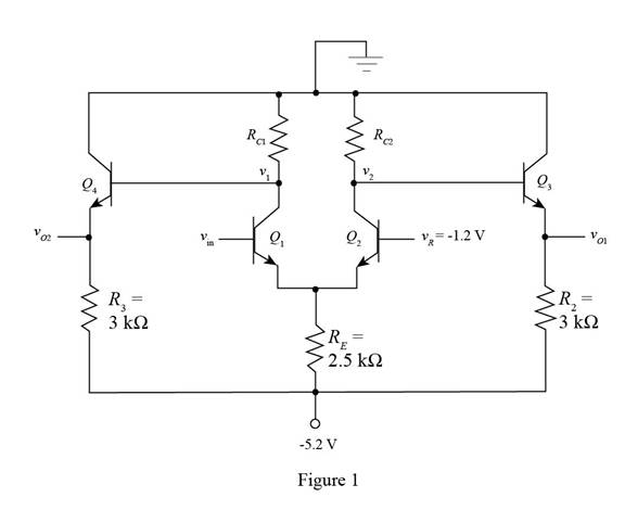
The given diagram is shown in Figure 1
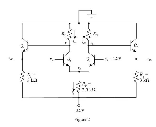
Mark the currents and redraw the circuit.
The required diagram is shown in Figure 2
The transistor number two is off and the value of the current
The expression for the value of the emitter voltage
Substitute
The expression for the value of the emitter current
Substitute
Substitute
The expression for the value of the capacitance of resistance
Substitute
Conclusion:
Therefore, the value of the resistance is
(b)
The value of the resistance
(b)
Answer to Problem 17.5P
The value of the resistance is
Explanation of Solution
Calculation:
The first transistor is on and the second is off.
The expression for the voltage
Substitute
The expression for the value of the emitter current
Substitute
The expression for the value of the current
Substitute
The expression for the value of the resistance
Substitute
Conclusion:
Therefore, the value of the resistance is
(c)
The value of the output voltage
(c)
Answer to Problem 17.5P
The case when the input voltage is
Explanation of Solution
Calculation:
Consider the case when the input voltage is
The expression to determine the value of the voltage
Substitute
The expression to determine the value of the voltage
Substitute
Consider the case when the input voltage is
The expression to determine the value of the voltage
Substitute
The expression to determine the value of the voltage
Substitute
Conclusion:
Therefore, the case when the input voltage is
(d)
The expression for the power dissipated in the circuit.
(d)
Answer to Problem 17.5P
The value of the power dissipated in the circuit for the input voltage
Explanation of Solution
Calculation:
Consider the case when the input voltage is
The expression for the value of the current through the resistance
Substitute
The expression for the value of the current through the resistance
Substitute
The expression for the value of the power dissipated in the circuit is given by,
Substitute
Consider the case when the input voltage is
The expression for the value of the current through the resistance
Substitute
The expression for the value of the current through the resistance
Substitute
The expression for the value of the power dissipated in the circuit is given by,
Substitute
Conclusion:
Therefore, the value of the power dissipated in the circuit for the input voltage
Want to see more full solutions like this?
Chapter 17 Solutions
Microelectronics: Circuit Analysis and Design


- For a PCM system with the following parameters, Parameters: (i) Maximum analog input frequency = 5 kHz; (ii) Maximum decoded voltage at the receiver = ±5.01 V; (iii) Minimum dynamic range = 54 dB. (Use 2 decimal places) a) What is the coding efficiency in % b) What is the resolution in V? c) Determine the maximum quantization error in V.arrow_forwardFor a PCM system with the following parameters, Parameters: (i) Maximum analog input frequency = 5 kHz; (ii) Maximum decoded voltage at the receiver = ±5.01 V; (iii) Minimum dynamic range = 54 dB. (Use 2 decimal places) a) What is the coding efficiency in % b) What is the resolution in V? c) Determine the maximum quantization error in V. d) Determine the minimum sampling rate in KHz e)Determine minimum number of bits use for the PCM code excluding sign bit.arrow_forwardDESIGN A 3 X8 DECODER CIRCUIT USING THE INTEGRATED CIRCUIT 74139 ( 2x4 DECODER) SO AS TO SATISFY THE FUNCTION F(A,B,C)= SUM ( 0,3,4,7).PLease I need answer within 10 minutesarrow_forward
- Develop the truth table and constellation diagram of QPSK using I -channel reference cos wct and 90 degrees phase shift for IQ inputs 00 and 10. Draw the analog output waveform of the given inputsarrow_forwardDraw and show the BFSK modulation waveform for the given binary data sequence “1,0,0,1”, and also draw its BFSK constellation diagram.arrow_forwardDraw the schematic of a three-input NAND gate. What are the W/L ratios for thetransistors based?arrow_forward
- What is the term used to express the ability of a measuring system to maintain its standard performance? a) Zero Reliabilityb) Stabilitye) Sensitivityd) Linearityarrow_forwardState the advantages and disadvantages of theDSB_LCarrow_forwardCourse: Data Networks - ECTE201 Outline Digital-to-analog conversion between sender and receiver with analog.arrow_forward
- 20] How long does it take a 3.3uF Capacitor to fully charge through a 18k Ohm Resistor? Express your answer in Decimal with 2 digits of significance. 21] What is the minimum Sum-of-Products equation for the Function 'Y = BAC + F + BC'? 22] Implement the Function 'Y = ACB + BC + E' using a 4-Input, 2-Address Bit Multiplexer. What are the Equations for the Multiplexer Data Inputs (D3 - D0)?arrow_forwardBy using BPSK modulation from a communication channel, voice transmission is made at a data rate of 240 kbps. However, due to the low speed, it is desired to increase this rate to 3*240 kbps, but to keep the bandwidth constant while this process is being done. In order to do this, which and how many levels of modulation should be preferred. ( Binary data rate of 3 * 240 kbps transmitted per second, symbol rate should be obtained to provide the same bandwidth as modulation.)arrow_forwardAssess the method to generate a 6.25 MHz signal using a 10-bits serial shift register operated with 50 MHz clock. Show all the necessary steps, delay calculations and workings in your answer.arrow_forward
 Introductory Circuit Analysis (13th Edition)Electrical EngineeringISBN:9780133923605Author:Robert L. BoylestadPublisher:PEARSON
 Delmar's Standard Textbook Of ElectricityElectrical EngineeringISBN:9781337900348Author:Stephen L. HermanPublisher:Cengage Learning
 Programmable Logic ControllersElectrical EngineeringISBN:9780073373843Author:Frank D. PetruzellaPublisher:McGraw-Hill Education
 Fundamentals of Electric CircuitsElectrical EngineeringISBN:9780078028229Author:Charles K Alexander, Matthew SadikuPublisher:McGraw-Hill Education
 Electric Circuits. (11th Edition)Electrical EngineeringISBN:9780134746968Author:James W. Nilsson, Susan RiedelPublisher:PEARSON
 Engineering ElectromagneticsElectrical EngineeringISBN:9780078028151Author:Hayt, William H. (william Hart), Jr, BUCK, John A.Publisher:Mcgraw-hill Education,