
Concept explainers
Videos
Assume
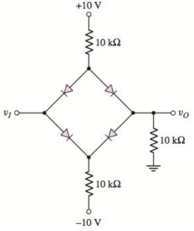
Figure P2.51
To plot: The output voltage,
Explanation of Solution
Given:
Calculation:
Case 1:
Assume that diodes
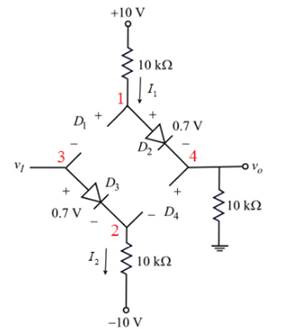
Figure 1
Apply the Kirchhoff’s voltage to the outer branch of the circuit shown in figure 1.
Therefore,
The voltage at node
The voltage at node
Apply the Kirchhoff’s voltage to the input branch of the circuit shown in figure
Therefore,
The voltage at node
The diode
The diode
Therefore, diodes
The output voltage is constant for
Case 2:
Assume that diodes
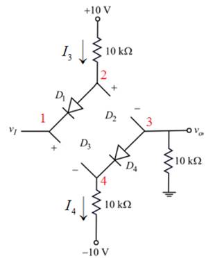
Figure 2
Apply the Kirchhoff’s voltage to the outer branch of the circuit shown in figure 2.
The voltage at node
The voltage at node
Apply the Kirchhoff’s voltage to the input branch of the circuit shown in figure 2.
Therefore,
The voltage at node
The diode
The diode
Therefore, diodes
Therefore, the output voltage is constant for
Case 3:
Assume that diodes
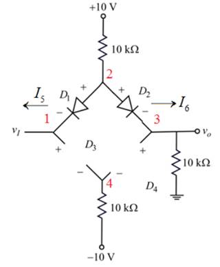
Figure 3
Apply the Kirchhoff’s current law at node
The diode
Apply the Kirchhoff’s voltage law to the input branch of the circuit shown in figure 3.
The voltage across diode
Consider equation(1).
Rewrite as,
Therefore, the output voltage is,
Therefore, plot
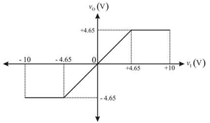
Conclusion:
Therefore, plot of
Want to see more full solutions like this?
Chapter 2 Solutions
Microelectronics: Circuit Analysis and Design


- What is CEMF?arrow_forwardCalculate diode forward current IF, diode voltage VF, and voltage drop across series resistor for three diode models (ideal, practical and complex).Assume diode forward resistance (dynamic resistance) r’d = 25Ω. Reverse leakage current IR = 75 nanoA with series resistance of RL = 100kΩ in reverse bias. Draw equivalent circuit diagrams of each model separately and plot corresponding I/V characteristics for each model.arrow_forward2-2VOLTAGE-CURRENT CHARACTERISTICOF A DIODE 1.Explain how to generate the forward-bias portion of the characteristic curve. 2.What would cause the barrier potential of a silicon diode to decrease from 0.7 V to 0.6 V?arrow_forward
- Draw sketches to illustrate the behaviour of the following: i. Reverse Biased Zener Diode ii. Ideal Diode iii. Forward Biased Practical Diode iv. Equivalent circuit of a simple diode circuit v. Practical Diode at Average AC Resistance Levelarrow_forwardFor the values of R1=230, R2=230, R3=400, Vs=15. If the real diode (offset voltage=0.7V) were conduxting, then the value of voltage source Vb should be? solve correct or will dislikearrow_forwardConsider a Zener diode in the figure given below where, V1 = 30 V. Determine the Zener current IZ if RZ = 100 Ω.arrow_forward
- In one graph, sketch the I-V curve for the forward bias. Forward Bias of PN Junction Diode:1. The Cut in Voltage or Knee Voltage of 1N4148 is _____________Volts.2. The Static Forward resistance of 1N4148 is __________________ .arrow_forwardConsider the circuit in Figure 2–75 .(a) What type of circuit is this?(b) What is the total peak secondary voltage?(c) Find the peak voltage across each half of the secondary.(d) Sketch the voltage waveform across RL.(e) What is the peak current through each diode?(f) What is the PIV for each diode?arrow_forwardQ2:- Find the level of Vo for each circuit shown in the Figure below. Also, determine the status of each diode; if it is forward or reverses biasing. Assume all diodes are silicone with 0.7v drop.arrow_forward
- Determine the Q-points for the diode in the circuit given below using the constant voltage drop model with Von = 0.7 V, where R1 = 44 kΩ and R2 = 23 kΩ.arrow_forward2-1 DIODE OPERATION 1.To forward-bias a diode, to which region must the positive terminal of a voltage source be connected? 2.Explain why a series resistor is necessary when a diode is forward-biased. 3.How much reverse-bias voltage can be applied to a diode? 4.Define the avalanche effect.arrow_forward1- Connect the Diode Characteristics circuit with a 800 resistor and anvariable AC input voltage source.2- Draw the readings on a V vs I curve and the two graphs look as followsForward bias and reverse bias graph.3- draw the output voltage cross the diode.4- Discuss the diode I-V characteristics curvearrow_forward

 Electricity for Refrigeration, Heating, and Air C...Mechanical EngineeringISBN:9781337399128Author:Russell E. SmithPublisher:Cengage Learning
 Delmar's Standard Textbook Of ElectricityElectrical EngineeringISBN:9781337900348Author:Stephen L. HermanPublisher:Cengage Learning