
Videos
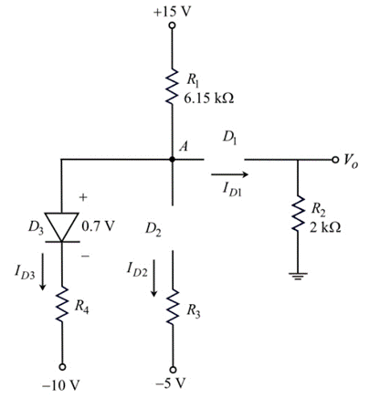
The cut−in voltage of each diode in the circuit shown in Figure P2.52 is
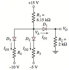
Figure P2.52
(a)
The values of
Answer to Problem 2.52P
The current flowing through diodes is
Explanation of Solution
Given:
Calculation:
The cut-in voltage for each diode is,
Assume all diodes are ON.
Draw the circuit diagram with node voltages and cut-in voltages.
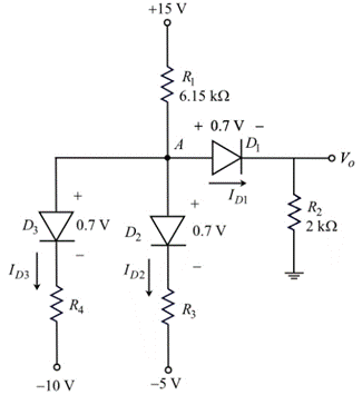
Apply Kirchhoff’s current law node A.
Substitute
Therefore, the voltage at node
Calculate the current flowing through diode,
Substitute
Therefore, the current flowing through diode
Calculate the current flowing through diode,
Substitute
Therefore, the current flowing through diode
Calculate the current flowing through diode,
Substitute
Therefore, the current flowing through diodes is
Conclusion:
Therefore, the current flowing through diodes is
(b)
The values of
Answer to Problem 2.52P
The current flowing through diodes is
Explanation of Solution
Given:
Calculation:
Assume diode
Draw the circuit diagram with node voltages and cut-in voltages.
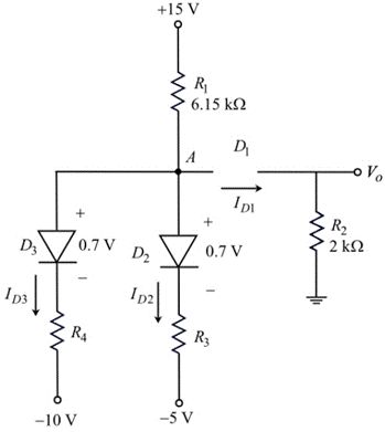
Apply Kirchhoff’s current law node A.
Substitute
Therefore, the voltage at node
The diode
That is,
Therefore, the current flowing through diode
Calculate the current flowing through diode,
Substitute
Therefore, the current flowing through diode
Calculate the current flowing through diode,
Substitute
Therefore, the current flowing through diode
Conclusion:
Therefore, the current flowing through diodes is
(c)
The values of
Answer to Problem 2.52P
The current flowing through diodes is
Explanation of Solution
Given:
Calculation:
Assume diode
Draw the circuit diagram with node voltages and cut-in voltages.
Apply Kirchhoff’s current law node A.
Substitute
Therefore, the voltage at node
The Diode
That is,
Therefore, the current flowing through diode
The current flowing through the diode,
That is,
Therefore, the current flowing through diode
Calculate the current flowing through diode,
Substitute
Therefore, the current flowing through diode
Conclusion:
Therefore, the current flowing through diodes is
Want to see more full solutions like this?
Chapter 2 Solutions
Microelectronics: Circuit Analysis and Design


- 2.13 Two diodes are connected in series as shown in Figure 2.11a to share a total de reverse volt age of VD=5 KV. The reverse leakage currents of two diode I=25 mA, 1,2 = 30 mA. (a) Find the diode voltage if the voltage sharing resistances R₁ and R₂ are equal R₁ = R₂ = 200 KN. (b) Find the voltage sharing resistance R₁ and R₂ if the diode voltage are equal Vd1= Vd2= Vd/2arrow_forwardDiodesFill in the blanks with the words belowcheck valve, conductance, convert, crystalline, impurities, infinite, galena, p–n junction, rectifying,resistance, selenium, semiconductor, switching circuits, tailored, temperature, threshold, two-terminal,unidirectionalA diode is a 1 ………………… electronic component that conducts current primarily in one direction(asymmetric 2 ………………..); it has low (ideally zero) 3 ……………… in one direction, and high (ideally4 ………………..) resistance in the other. A 5 ………….. diode, the most common type today, is a 6……….. piece of semiconductor material with a 7 ………………. connected to two electrical terminals. Avacuum tube diode has two electrodes, a plate (anode) and a heated cathode. Semiconductor diodes were thefirst semiconductor electronic devices. The discovery of crystals' 8 ……………… abilities was made byGerman physicist Ferdinand Braun in 1874. The first semiconductor diodes, developed around 1906, weremade of mineral crystals such as 9 ……………….. . Today,…arrow_forwardIn the circuit, diode D1 has n = 1.4 and has an operating point I D = 1mA at V D =0.7 V and is at room temperature. Diode D2 has an area that is 20 times larger than D1 but isotherwise the same. a) What is the current through diode D1?b) What is the value of the saturation current, Is for diode D2?c) What is the voltage Vx ? d) Determine the value of R to make Vo = -0.2Varrow_forward
- Fill in the blanks with the words belowcheck valve, conductance, convert, crystalline, impurities, infinite, galena, p–n junction, rectifying,resistance, selenium, semiconductor, switching circuits, tailored, temperature, threshold, two-terminal,unidirectionalA diode is a 1 ………………… electronic component that conducts current primarily in one direction(asymmetric 2 ………………..); it has low (ideally zero) 3 ……………… in one direction, and high (ideally4 ………………..) resistance in the other. A 5 ………….. diode, the most common type today, is a 6……….. piece of semiconductor material with a 7 ………………. connected to two electrical terminals. Avacuum tube diode has two electrodes, a plate (anode) and a heated cathode. Semiconductor diodes were thefirst semiconductor electronic devices. The discovery of crystals' 8 ……………… abilities was made byGerman physicist Ferdinand Braun in 1874. The first semiconductor diodes, developed around 1906, weremade of mineral crystals such as 9 ……………….. . Today, most…arrow_forwardFor the ideal-diode clipper circuit given below, VS = 12.sinωt V. Determine the output voltage Vout and sketch this function. Remove the short circuit between points x and y, and replace it with a 2kΩ Resistor. Find the range of values of VS for; D1 and D2 are OFF D1 is ON and D2 is OFF D1 is OFF and D2 is ON Is it possible for both D1 and D2 to be ON?arrow_forwardDiodes D1, D2, D3 and D4 are identical Silicon diodes with forward voltage drop of 0.7volts. Consider vi to be the circuit's input voltage.A) Under what input conditions will diode D1 conduct? B) If D1 is conducting, express vo in terms of vi. C) Under what conditions will diode D4 conduct? D) If D4 is conducting, express vo in terms of vi. E) Under what input conditions will none of the diodes be conducting? F) If none of the diodes are conducting, what is vo? G) The input to the circuit has the waveform shown below. Plot the waveform of thevoltage vo. Show all the important quantities in your plot.arrow_forward
- 4. a. Using the approximate characteristics for the Si diode, determine V D , I D , and V R for thecircuit of Fig. 2.154 .b. Perform the same analysis as part (a) using the ideal model for the diode.c. Do the results obtained in parts (a) and (b) suggest that the ideal model can provide a goodapproximation for the actual response under some conditions?arrow_forwardFor the half-wave rectifier circuit shown, the diode is not ideal and is modeled as an ideal voltage source of value Vf= 0.65V in series with an ideal diode. Vin= 5sin(2π100t) and R =510Ω. What is the output voltage at time t=24mst=24ms? 2- For the same circuit as in Question 1, what is the output voltage at time t=35.4ms t=35.4ms? Enter your answer in volts 3- For the same circuit as in Question 1, what is the magnitude of the diode current at time t=12mst=12ms? Enter your answer in mA without units.arrow_forwardFor the half-wave rectifier circuit shown, the diode is not ideal and is modeled as an ideal voltage source of value Vf= =0.65V in series with an ideal diode. Vin= 2sin(2π10t) and R= 470Ω. What is the magnitude of the diode current at time t=60mst=60ms? 2- At what time between 0and T/4 seconds is the magnitude of the diode current equal to 2.66mA? Tis the period of Vin Enter your answer in millisecondsarrow_forward
- 4 - The figure below shows a part of the energy band diagram of a p-n semiconductor junction. According to the situation shown in the figure, in the equilibrium condition, we can identify the currents as follows: *image attached* ( ) i1:hole diffusion current, i2:electron drift current, i3:hole drift current and i4:electron diffusion current. ( ) i1:hole drift current, i2:electron diffusion current, i3:hole diffusion current and i4:electron drift current. ( ) i1:electron diffusion current, i2:electron diffusion current, i3:hole drift current and i4:hole drift current. ( ) i1:electron drift current, i2:electron diffusion current, i3:hole diffusion current and i4:hole drift current. ( ) i1:hole drift current, i2:electron drift current, i3:hole diffusion current and i4:electron diffusion current.arrow_forwardGiven the schematic below, assume D1 and D2 are silicon with forward voltages of 0.7V. Find the following (with solutions) a) Conditions required wherein none of the diodes are conducting b) If both diodes are not conduction, what is Vo? Express in terms of Vi c) Plot the overall relationship of Vo and Vi in the coordinate system shown below. Remember, you are to plot the transfer characteristics of the circuit.arrow_forwardi) The equation above contains really only three variables in it: Id, Vd, and T. All the other terms are constants. Since in most cases we assume temperature is fairly constant as well, we are really only dealing with two variables: diode current and diode voltage. Based on this realization, re-write the equation as proportionality rather than equality, showing how the two variables of diode current and voltage relate ii) Based on this simplified equation, what would an I vs V graph for a PN junction look like? How does this graph compare against the I vs V graph for a resistor? iii) When "P" and "N" type semiconductor pieces are brought into close contact, free electrons from the "N" piece will rush over to fill holes in the "P" piece, creating a zone on both sides of the contact region devoid of charge carriers. What is this zone called, and what are its electrical characteristics? iv) What happens to the thickness of the region in a PN junction (answer above) when an external…arrow_forward
 Introductory Circuit Analysis (13th Edition)Electrical EngineeringISBN:9780133923605Author:Robert L. BoylestadPublisher:PEARSON
 Delmar's Standard Textbook Of ElectricityElectrical EngineeringISBN:9781337900348Author:Stephen L. HermanPublisher:Cengage Learning
 Programmable Logic ControllersElectrical EngineeringISBN:9780073373843Author:Frank D. PetruzellaPublisher:McGraw-Hill Education
 Fundamentals of Electric CircuitsElectrical EngineeringISBN:9780078028229Author:Charles K Alexander, Matthew SadikuPublisher:McGraw-Hill Education
 Electric Circuits. (11th Edition)Electrical EngineeringISBN:9780134746968Author:James W. Nilsson, Susan RiedelPublisher:PEARSON
 Engineering ElectromagneticsElectrical EngineeringISBN:9780078028151Author:Hayt, William H. (william Hart), Jr, BUCK, John A.Publisher:Mcgraw-hill Education,