Microelectronics: Circuit Analysis and Design
4th Edition
ISBN: 9780073380643
Author: Donald A. Neamen
Publisher: McGraw-Hill Companies, The
bartleby

Videos

Textbook Question
Book Icon
Chapter 3, Problem 3.3CAE

Consider the NMOS circuit shown in Figure 3.36. Plot the voltage transfer characteristics, using a PSpice simulation. Use transistor parameters similar to those in Example 3.9. What are the values of V O for V I = 1.5 V and V I = 5 V ?

Expert Solution & Answer
Check Mark
To determine

To plot: Thevoltage transfer characteristics using PSpice simulation.

To find: The value of output voltage for the given input voltage.

Answer to Problem 3.3CAE

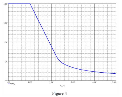
The required plot is shown in Figure 4 and the output voltage for the input voltage of 1.5V is 2.88V and the value of the output voltage for the input voltage of 5V is 0.349V .

Explanation of Solution

Given:

The required diagram with the values marked is shown in Figure 1.
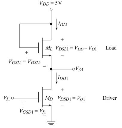
  Microelectronics: Circuit Analysis and Design, Chapter 3, Problem 3.3CAE , additional homework tip  1

Figure 1

Calculation:

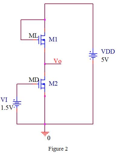
Draw the PSpice equivalent circuit with all the values marked.

  Microelectronics: Circuit Analysis and Design, Chapter 3, Problem 3.3CAE , additional homework tip  2

The snip for the drop box with all the setting is shown in Figure 3

  Microelectronics: Circuit Analysis and Design, Chapter 3, Problem 3.3CAE , additional homework tip  3

Left click on the trace option and then click on add trace and type “V(Vo)”command in trace expression box to obtain the voltage transfer characteristic of the inverter.

The required characteristic diagram is shown in Figure 4

  Microelectronics: Circuit Analysis and Design, Chapter 3, Problem 3.3CAE , additional homework tip  4

Consider the input voltage is 1.5V .

The expression for the current IDD1 is given by,

  IDD1=KnD(V GSD1V TND)2

The expression for the current IDL1 is given by,

  IDL1=KnL(V GSL1V TNL)2

The expression for the value of the voltage VGSL1 is evaluated as,

  VGSD1=VI1VDSD1=VO1VGSL1=VDSL1VGSL1=VDDVO1

The expression for the current IDD1 is given by,

  IDD1=IDL1

Substitute VI1 for VGSD1 , VDDVO1 for VGSL1 , KnL(V GSL1V TNL)2 for IDL1 and KnD(V GSD1V TND)2 for IDD1 in the above equation.

  KnD(V I1V TND)2=KnL(V DDV O1V TNL)2

Substitute 5V for VDD ,, 1.5V for VI1 , 1V for VTND , 1V for VTNL , 50μA/V2 for KnD , and 10μA/V2 for KnL in the above equation.

  50μA/V2(1.5V1V)2=10μA/V2(5V V O11V)2( V O1)28VO1+14.75=0VO1=2.88V,5.11V

The input voltage is just 1.5V so the output voltage is 2.88V .

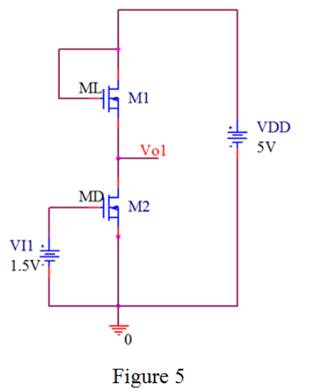
Draw the PSpice circuit for the figure 1 with the input voltage of 1.5V .

The required diagram is shown in Figure 5

  Microelectronics: Circuit Analysis and Design, Chapter 3, Problem 3.3CAE , additional homework tip  5

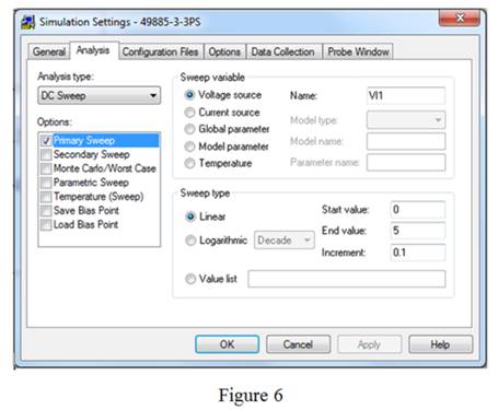
The simulation settings for the circuit is shown in Figure 6

  Microelectronics: Circuit Analysis and Design, Chapter 3, Problem 3.3CAE , additional homework tip  6

The simulated circuit for Figure 5 with the output voltage is shown in Figure 7

  Microelectronics: Circuit Analysis and Design, Chapter 3, Problem 3.3CAE , additional homework tip  7

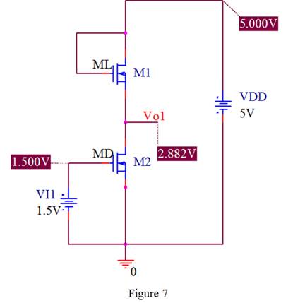
Thus, the value of the simulated output voltage is same as the theoretical output voltage.

Consider the input voltage is 5V .

Mark the values and draw the circuit for the input voltage of 5V .

The required diagram is shown in Figure 8

  Microelectronics: Circuit Analysis and Design, Chapter 3, Problem 3.3CAE , additional homework tip  8

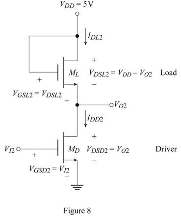
The values of different voltage are,

  VGSD2=VI2VDSD2=VO2VGSL2=VDSL2VGSL2=VDDVO2

The driver transistor is biased in non-saturation region as the drain to source voltage is very large. So the expression for the relation of the drain currents is given by,

  IDD2=IDL2

The expression for IDD2 in non-saturation region is given as,

  IDD2=KnD[2(VGSD2VTND)VDS2( V DS2)2]

The load transistor is in the saturation region and the drain current is given by,

  IDL2=KnL[VDSL2VTNL]2

By the relation IDD2=IDL2 ,

  KnD[2( V GSD2 V TND)VDS2( V DS2 )2]=KnL[V DSL2V TNL]2KnD[2( V I2 V TND)VO2( V O2 )2]=KnL[V DDV O2V TNL]2

The value of the output voltage is evaluated as,

  50μA/V2[2(5V1V)VO2( V O2 )2]=10μA/V2[5VV O21V]26( V O2)248VO2+16=0VO2=7.65V,0.3485VVO2=0.349V

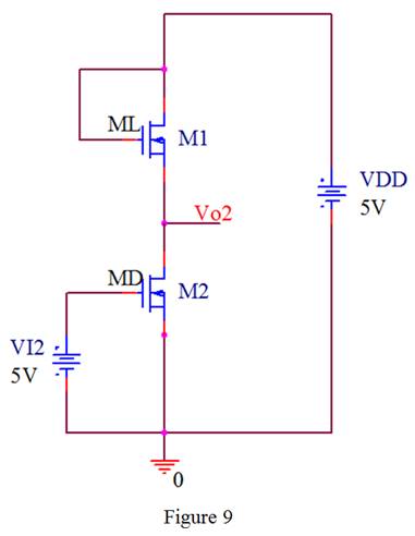
The simulation circuit for Figure 8 is shown in Figure 9

  Microelectronics: Circuit Analysis and Design, Chapter 3, Problem 3.3CAE , additional homework tip  9

The output of the simulated circuit for the above circuit is shown in Figure 11

  Microelectronics: Circuit Analysis and Design, Chapter 3, Problem 3.3CAE , additional homework tip  10

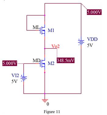
Thus, the output voltage of 0.349V is verified.

Conclusion:

Therefore, the required plot is shown in Figure 4 and the output voltage for the input voltage of 1.5V is 2.88V and the value of the output voltage for the input voltage of 5V is 0.349V .

Want to see more full solutions like this?

Subscribe now to access step-by-step solutions to millions of textbook problems written by subject matter experts!
Students have asked these similar questions
Explain the concept of a very large-scale integrated circuit (VLSI).
Describe the basic principle of operation of a bipolar junction transistor. Include explanation for the following : When minority carriers flow across the transistor Why the collector current is almost unaffected by the collector potential
Briefly explain Effects of Gate Length (L) and Oxide Thickness on MOSFET drain current with figure/graph.

Chapter 3 Solutions

Microelectronics: Circuit Analysis and Design

Ch. 3 - For the transistor in the circuit in Figure 3.28,...Ch. 3 - Consider the circuit shown in Figure 3.30. The...Ch. 3 - Consider the circuit in Figure 3.30. Using the...Ch. 3 - (a) Consider the circuit shown in Figure 3.33. The...Ch. 3 - Consider the NMOS inverter shown in Figure 3.36...Ch. 3 - Consider the circuit shown in Figure 3.39 with...Ch. 3 - Consider the circuit in Figure 3.41. Assume the...Ch. 3 - Prob. 3.7TYUCh. 3 - Consider the circuit in Figure 3.43. The...Ch. 3 - For the circuit shown in Figure 3.36, use the...Ch. 3 - Consider the circuit shown in Figure 3.44. The...Ch. 3 - For the circuit shown in Figure 3.39, use the...Ch. 3 - For the MOS inverter circuit shown in Figure 3.45,...Ch. 3 - For the circuit in Figure 3.46, assume the circuit...Ch. 3 - The circuit shown in Figure 3.45 is biased at...Ch. 3 - The transistor in the circuit shown in Figure 3.48...Ch. 3 - In the circuit in Figure 3.46, let RD=25k and...Ch. 3 - For the circuit shown in Figure 3.49(a), assume...Ch. 3 - Prob. 3.15EPCh. 3 - Consider the constantcurrent source shown in...Ch. 3 - Consider the circuit in Figure 3.49(b). Assume...Ch. 3 - Consider the circuit shown in Figure 3.50. Assume...Ch. 3 - The transistor parameters for the circuit shown in...Ch. 3 - The transistor parameters for the circuit shown in...Ch. 3 - The parameters of an nchannel JFET are IDSS=12mA ,...Ch. 3 - The transistor in the circuit in Figure 3.62 has...Ch. 3 - For the pchannel transistor in the circuit in...Ch. 3 - Consider the circuit shown in Figure 3.66 with...Ch. 3 - The nchannel enhancementmode MESFET in the circuit...Ch. 3 - For the inverter circuit shown in Figure 3.68, the...Ch. 3 - Describe the basic structure and operation of a...Ch. 3 - Sketch the general currentvoltage characteristics...Ch. 3 - Describe what is meant by threshold voltage,...Ch. 3 - Describe the channel length modulation effect and...Ch. 3 - Describe a simple commonsource MOSFET circuit with...Ch. 3 - Prob. 6RQCh. 3 - In the dc analysis of some MOSFET circuits,...Ch. 3 - Prob. 8RQCh. 3 - Describe the currentvoltage relation of an...Ch. 3 - Describe the currentvoltage relation of an...Ch. 3 - Prob. 11RQCh. 3 - Describe how a MOSFET can be used to amplify a...Ch. 3 - Describe the basic operation of a junction FET.Ch. 3 - Prob. 14RQCh. 3 - (a) Calculate the drain current in an NMOS...Ch. 3 - The current in an NMOS transistor is 0.5 mA when...Ch. 3 - The transistor characteristics iD versus VDS for...Ch. 3 - For an nchannel depletionmode MOSFET, the...Ch. 3 - Verify the results of Example 3.4 with a PSpice...Ch. 3 - The threshold voltage of each transistor in Figure...Ch. 3 - The threshold voltage of each transistor in Figure...Ch. 3 - Consider an nchannel depletionmode MOSFET with...Ch. 3 - Determine the value of the process conduction...Ch. 3 - An nchannel enhancementmode MOSFET has parameters...Ch. 3 - Consider the NMOS circuit shown in Figure 3.36....Ch. 3 - An NMOS device has parameters VTN=0.8V , L=0.8m ,...Ch. 3 - Consider the NMOS circuit shown in Figure 3.39....Ch. 3 - A particular NMOS device has parameters VTN=0.6V ,...Ch. 3 - MOS transistors with very short channels do not...Ch. 3 - For a pchannel enhancementmode MOSFET, kp=50A/V2 ....Ch. 3 - For a pchannel enhancementmode MOSFET, the...Ch. 3 - The transistor characteristics iD versus SD for a...Ch. 3 - A pchannel depletionmode MOSFET has parameters...Ch. 3 - Calculate the drain current in a PMOS transistor...Ch. 3 - sDetermine the value of the process conduction...Ch. 3 - Enhancementmode NMOS and PMOS devices both have...Ch. 3 - For an NMOS enhancementmode transistor, the...Ch. 3 - The parameters of an nchannel enhancementmode...Ch. 3 - An enhancementmode NMOS transistor has parameters...Ch. 3 - An NMOS transistor has parameters VTO=0.75V ,...Ch. 3 - (a) A silicon dioxide gate insulator of an MOS...Ch. 3 - In a power MOS transistor, the maximum applied...Ch. 3 - In the circuit in Figure P3.26, the transistor...Ch. 3 - The transistor in the circuit in Figure P3.27 has...Ch. 3 - Prob. D3.28PCh. 3 - The transistor in the circuit in Figure P3.29 has...Ch. 3 - Consider the circuit in Figure P3.30. The...Ch. 3 - For the circuit in Figure P3.31, the transistor...Ch. 3 - Design a MOSFET circuit in the configuration shown...Ch. 3 - Consider the circuit shown in Figure P3.33. The...Ch. 3 - The transistor parameters for the transistor in...Ch. 3 - For the transistor in the circuit in Figure P3.35,...Ch. 3 - Design a MOSFET circuit with the configuration...Ch. 3 - The parameters of the transistors in Figures P3.37...Ch. 3 - For the circuit in Figure P3.38, the transistor...Ch. 3 - Prob. 3.39PCh. 3 - Prob. 3.40PCh. 3 - Design the circuit in Figure P3.41 so that...Ch. 3 - Prob. 3.42PCh. 3 - Prob. 3.43PCh. 3 - Prob. 3.44PCh. 3 - Prob. 3.45PCh. 3 - Prob. 3.46PCh. 3 - Prob. 3.47PCh. 3 - The transistors in the circuit in Figure 3.36 in...Ch. 3 - For the circuit in Figure 3.39 in the text, the...Ch. 3 - Prob. 3.50PCh. 3 - The transistor in the circuit in Figure P3.51 is...Ch. 3 - Prob. 3.52PCh. 3 - For the twoinput NMOS NOR logic gate in Figure...Ch. 3 - All transistors in the currentsource circuit shown...Ch. 3 - All transistors in the currentsource circuit shown...Ch. 3 - Consider the circuit shown in Figure 3.50 in the...Ch. 3 - The gate and source of an nchannel depletionmode...Ch. 3 - For an nchannel JFET, the parameters are IDSS=6mA...Ch. 3 - A pchannel JFET biased in the saturation region...Ch. 3 - Prob. 3.60PCh. 3 - Prob. 3.61PCh. 3 - The threshold voltage of a GaAs MESFET is...Ch. 3 - Prob. 3.63PCh. 3 - Prob. 3.64PCh. 3 - Prob. 3.65PCh. 3 - For the circuit in Figure P3.66, the transistor...Ch. 3 - Prob. 3.67PCh. 3 - Prob. 3.68PCh. 3 - For the circuit in Figure P3.69, the transistor...Ch. 3 - Prob. 3.70PCh. 3 - Prob. 3.71PCh. 3 - Prob. 3.72PCh. 3 - Using a computer simulation, verify the results of...Ch. 3 - Consider the PMOS circuit shown in Figure 3.30....Ch. 3 - Consider the circuit in Figure 3.39 with a...Ch. 3 - Prob. D3.79DPCh. 3 - Consider the multitransistor circuit in Figure...
Knowledge Booster
Background pattern image
Electrical Engineering
Learn more about
Need a deep-dive on the concept behind this application? Look no further. Learn more about this topic, electrical-engineering and related others by exploring similar questions and additional content below.
Similar questions
SEE MORE QUESTIONS
Recommended textbooks for you
Text book image
Introductory Circuit Analysis (13th Edition)
Electrical Engineering
ISBN:9780133923605
Author:Robert L. Boylestad
Publisher:PEARSON
Text book image
Delmar's Standard Textbook Of Electricity
Electrical Engineering
ISBN:9781337900348
Author:Stephen L. Herman
Publisher:Cengage Learning
Text book image
Programmable Logic Controllers
Electrical Engineering
ISBN:9780073373843
Author:Frank D. Petruzella
Publisher:McGraw-Hill Education
Text book image
Fundamentals of Electric Circuits
Electrical Engineering
ISBN:9780078028229
Author:Charles K Alexander, Matthew Sadiku
Publisher:McGraw-Hill Education
Text book image
Electric Circuits. (11th Edition)
Electrical Engineering
ISBN:9780134746968
Author:James W. Nilsson, Susan Riedel
Publisher:PEARSON
Text book image
Engineering Electromagnetics
Electrical Engineering
ISBN:9780078028151
Author:Hayt, William H. (william Hart), Jr, BUCK, John A.
Publisher:Mcgraw-hill Education,
How a MOSFET Works - with animation! | Intermediate Electronics; Author: CircuitBread;https://www.youtube.com/watch?v=Bfvyj88Hs_o;License: Standard Youtube License