
Videos
For the circuit in Figure P6.54, the parameters are
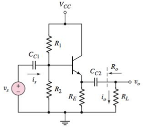
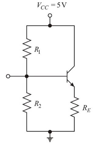
Figure P6.54
(a)
The value of
Answer to Problem 6.54P
The values of resistances are:
Explanation of Solution
Given:
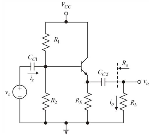
Given circuit:
Given Data:
Calculation:
Considering the BJT (Bipolar Junction Transistor) as single node, then, by Kirchhoff’s current law, the quiescent emitter current
In CE mode:
The quiescent collector current
DC analysis of given circuit
(Reducing the ac source

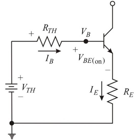
The Thevenin resistance
(Shorting the voltage source)
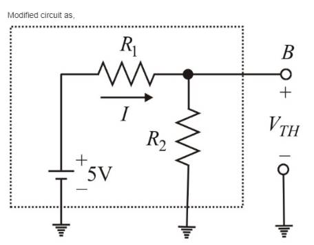
Therefore, the Thevenin voltage from the above circuit,
Using the equation (3),
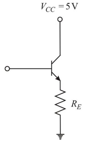
Modified circuit as,

Applying Kirchhoff’s voltage law around the collector-emitter loop as,
To calculate the value of
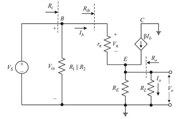
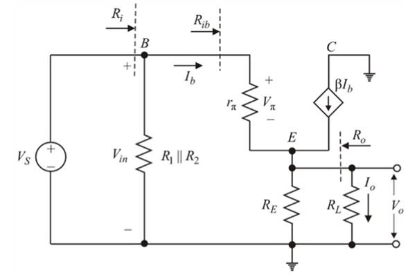
Small-signal analysis of given circuit
(Reducing the dc source to zero and the capacitors to short)
Diffusion resistance
The input resistance
Small signal current gain
Given the small signal current gain
Modified circuit as,

The Thevenin network is shown in above figure and
Kirchhoff's voltage law in the base-emitter loop as,
From equations (5), (8) and (9)
Combining equations (3), (4) and (10)
From equations (3) and (11)
Finding the output resistance
(b)
The current gain.
Answer to Problem 6.54P
The current gain for
Explanation of Solution
Given:
Given circuit:

Given Data:
Calculation:
Considering the BJT (Bipolar Junction Transistor) as single node, then, by Kirchhoff’s current law, the quiescent emitter current
In CE mode:
The quiescent collector current
DC analysis of given circuit
(Reducing the ac source
The Thevenin resistance
(Shorting the voltage source)

Therefore, the Thevenin voltage from the above circuit,
Using equation (3),
Modified circuit as,
Applying Kirchhoff’s voltage law around the collector-emitter loop as,
To calculate the value of
Small-signal analysis of given circuit
(Reducing the dc source to zero and the capacitors to short)
Diffusion resistance
The input resistance
Small signal current gain
Given the small signal current gain
Modified circuit as,
The Thevenin network is shown in above figure and
Kirchhoff's voltage law in the base-emitter loop as,
From equations (5), (8) and (9)
Combining equations (3), (4) and (10)
From equations (3) and (11)
Finding the output resistance
Determining the Small signal current gain
With load resistance
Want to see more full solutions like this?
Chapter 6 Solutions
Microelectronics: Circuit Analysis and Design


- Trying to solve this MOSFET question but not sure how.(Given Answer:a) Av = -gm (ro|| RD)b)Av = -30.7 Ri = 20 kohm Ro = 7.67 kohm)arrow_forwardUsing an example of your choice, identify the conditions needed for mechanical resonance and measures that can be taken to prevent this from occurring.arrow_forwardCurrent and impedance levels of push-pull RF amplifier. Solid-state RF power amplifiers that provide more than 50 W or so must deal with very large currents, because the typical silicon RF BJT or PET cannot with-stand a DC collector voltage higher than about 40V. (Newer devices using materials such as silicon carbide can exceed this voltage limitation and provide greater power for the same current level.) Suppose a push-pull RF amplifier using a DC collector voltage of 36 V must provide a total peak RF output power of 200W. Typically, the AC "swing" (peak-to-peak AC excursion) of voltage at the collectors cannot exceed twice the DC power-supply voltage. (a) If each of the two devices in the push-pull amplifier delivers IOOW and has a peak-to-peak voltage of (2 x 36) = 72 V across its output terminals , what is the peak current I at the collector of each device, assuming . "d C(PK) smus01 al voltage and current? (b) At this current IC<PK >' how much series inductance L at a…arrow_forward
- I need to design a multi stage amplifier with the following specs:arrow_forwardCoonsider the common emitter amplifier shown in figure below. Assume a β of 100, VBE = 0.7V, VT = 25mA and VA = 100V. Draw an equivalent DC model and determine the rπ, transconductance (gm) and ro. Draw an equaivalent AC model using the small-signal model Find an expression for vbe and vo in terms of the input voltagearrow_forwardThe circuit as shown is called a quadrature oscillator. Derive an expression for its frequency of oscillation. What value of RF is required for sinusoidaloscillation (in terms of R)?arrow_forward
- What are the applications of power amplifiers?arrow_forwardWe examined the common source amplifier shown in the figure in the 5th experiment. The selection criterion of the input capacitance is XCin = 0.1Rin. Calculate the required input capacitance value, Cin , if an input signal with a frequency of 4 kHz is applied.arrow_forwardQuestion Perform an ac analysis. Represent the amplifier by its ac equivalent circuit and discuss the input resistance at the base and the output resistance. draw the circuit subject electrical devices and circuits.arrow_forward
 Introductory Circuit Analysis (13th Edition)Electrical EngineeringISBN:9780133923605Author:Robert L. BoylestadPublisher:PEARSON
 Delmar's Standard Textbook Of ElectricityElectrical EngineeringISBN:9781337900348Author:Stephen L. HermanPublisher:Cengage Learning
 Programmable Logic ControllersElectrical EngineeringISBN:9780073373843Author:Frank D. PetruzellaPublisher:McGraw-Hill Education
 Fundamentals of Electric CircuitsElectrical EngineeringISBN:9780078028229Author:Charles K Alexander, Matthew SadikuPublisher:McGraw-Hill Education
 Electric Circuits. (11th Edition)Electrical EngineeringISBN:9780134746968Author:James W. Nilsson, Susan RiedelPublisher:PEARSON
 Engineering ElectromagneticsElectrical EngineeringISBN:9780078028151Author:Hayt, William H. (william Hart), Jr, BUCK, John A.Publisher:Mcgraw-hill Education,