
Videos
For the circuit in Figure P7.21, the transistor parameters are
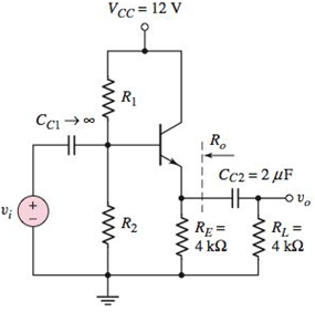
Figure P7.21
a.
To design: The bias stable circuit for the given condition.
Explanation of Solution
Given:
The circuit is given as:
IEQ =1.5mA.
The parameters of the circuit is given as:
The design needed for the bias stability is given as:
Recalling the general rule that the circuit is considered to be stable only, if:
Evaluating the Thevenin resistance
Substituting the known values in the equation:
Evaluating the value of base current
Substituting the known values in the above equation:
The expression for Thevenin s voltage
Substituting the known values in the above equation:
The other expression for Thevenin s voltage
Substituting the known values in the above equation:
The value of resistance
Substituting the known values in the above equation:
Therefore, the designed values are:
b.
The small signal mid band voltage gain.
Answer to Problem 7.21P
The value of voltage gain
Explanation of Solution
Given:
The circuit is given as:

IEQ =1.5mA.
The parameters of the circuit is given as:
Evaluating the value of collector current
Substituting the known values:
Evaluating the value of
Substituting the known values into the above equation:
Evaluating the value of output resistance
Substituting the known values into the above equation:
Evaluating the value of voltage gain
Substituting the known values into the above equation:
Therefore, the value of voltage gain
c.
The value of the output resistance.
Answer to Problem 7.21P
The value of output resistance
Explanation of Solution
Given:
The circuit is given as:

IEQ =1.5mA.
The parameters of the circuit is given as:
Evaluating the output resistance
Substituting the known values into the above equation:
Therefore, the value of output resistance
d.
The lower 3dB corner frequency for the given circuit.
Answer to Problem 7.21P
The value of lower corner frequency is 19.81Hz.
Explanation of Solution
Given:
The circuit is given as:

IEQ =1.5mA.
The parameters of the circuit is given as:
Evaluating the value of lower 3dB corner frequency:
Substituting the known values to the above equation:
Hence, the value of lower corner frequency is 19.81Hz.
Want to see more full solutions like this?
Chapter 7 Solutions
Microelectronics: Circuit Analysis and Design


- What are the advantages and disadvantages of single-sideband transmission? Briefly describe each.arrow_forwardExplain the basics of Double sideband supressed carrier signal and it's application. (Where it is being applied)arrow_forwardDescribe the general characteristics of the equivalent circuits that apply to the low frequency,midband,and high frequency ranges.arrow_forward
- A transistor has fT = 500 MHz and βF = 75.(a) What is the β-cutoff frequency fβ of this transistor? (b) to find an expression forthe frequency dependence of αF — that is, αF ( f ).[Hint: Write an expression for β(s).] What is theα-cutoff frequency for this transistor?arrow_forwardWhen does maximum frequency deviation occur in an FM signal? -It occurs during the transition of the modulating signal to the opposite sign. -It occurs at the maximum amplitude point of the modulating signal. -It occurs during the maximum rate of change of the modulating signal. -It occurs at the mean point of the modulating signal.arrow_forwardRegarding phase modulation (PM), an increase in the PM index, µ, results in an increase in the modulated signal’s bandwidth. (Explain) True Falsearrow_forward
- The Ebers-Moll model was one of the first mathematical models used to describe the characteristicsof the bipolar transistor. Show that the npn transportmodel equations can be transformed into the EbersMoll equations below. [Hint: Add and subtract 1from the collector and emitter current expressions.]arrow_forwardHow many channels are available in the 2.4 GHz band? List all the channels. What is the channelbandwidth?arrow_forward4. A modulated signal (AM) varies between the maximum values of +18V and -18V, if the carrier has an amplitude of 12V, a) What is the modulation index? b) What is the maximum magnitude of the modulator? c) Sketch the envelope of the modulated wavearrow_forward
 Introductory Circuit Analysis (13th Edition)Electrical EngineeringISBN:9780133923605Author:Robert L. BoylestadPublisher:PEARSON
 Delmar's Standard Textbook Of ElectricityElectrical EngineeringISBN:9781337900348Author:Stephen L. HermanPublisher:Cengage Learning
 Programmable Logic ControllersElectrical EngineeringISBN:9780073373843Author:Frank D. PetruzellaPublisher:McGraw-Hill Education
 Fundamentals of Electric CircuitsElectrical EngineeringISBN:9780078028229Author:Charles K Alexander, Matthew SadikuPublisher:McGraw-Hill Education
 Electric Circuits. (11th Edition)Electrical EngineeringISBN:9780134746968Author:James W. Nilsson, Susan RiedelPublisher:PEARSON
 Engineering ElectromagneticsElectrical EngineeringISBN:9780078028151Author:Hayt, William H. (william Hart), Jr, BUCK, John A.Publisher:Mcgraw-hill Education,