
Concept explainers
(a)
The maximum and the minimum value of the output voltage and the minimum corresponding input voltages for the circuit to operate in the linear region for given value of
(a)
Answer to Problem 8.20P
The maximum value of the output voltage is
Explanation of Solution
Calculation:
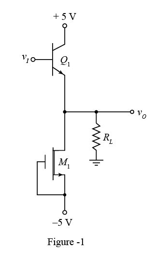
The given diagram is shown in Figure 1
The expression for the maximum value of the output voltage is given by,
Substitute
The expression for the drain to source saturation voltage is given by,
Substitute
The expression for the minimum value of the output voltage is given by,
Substitute
The expression for the minimum value of the input voltage is given by,
Substitute
The expression for the maximum value of the input voltage is given by,
Substitute
Conclusion:
Therefore, the maximum value of the output voltage is
(b)
The maximum and the minimum value of the output voltage and the minimum corresponding input voltages for the circuit to operate in the linear region for given value of
(b)
Answer to Problem 8.20P
The maximum value of the output voltage is
Explanation of Solution
Calculation:
The expression for the maximum value of the output voltage is given by,
Substitute
The expression for the drain to source saturation voltage is given by,
Substitute
The expression for the minimum value of the output voltage is given by,
Substitute
The expression for the minimum value of the input voltage is given by,
Substitute
The expression for the maximum value of the input voltage is given by,
Substitute
Conclusion:
Therefore, the maximum value of the output voltage is
(c)
The smallest value of the
(c)
Answer to Problem 8.20P
The minimum value of the load resistance is
Explanation of Solution
Calculation:
The expression for the current through the transistor
Substitute
The expression for the minimum value of the load resistance is
Substitute
The expression for the power delivered to the load is given by,
Substitute
The expression for the average power supplied by the source is given by,
Substitute
The expression for the value of power conversion efficiency is given by,
Substitute
Conclusion:
Therefore, the minimum value of the load resistance is
Want to see more full solutions like this?
Chapter 8 Solutions
Microelectronics: Circuit Analysis and Design


- The following parameters of NMOS used in the circuit in the figure are given. Al = NA K „= 100µA / V² 0 = Y C = 25 fF C, = 100 fF Accordingly; a) What is the cutoff frequency of the circuit? b) What is the upper cutoff frequency of the circuit?arrow_forwardThe topic is about BJT DC Analysis. Please show the correct and complete solution to this problem. Thank you!arrow_forwardThe bipolar differential amplifier as shown is biased by a 75-μA current source with an output resistance of 1MΩ. If the transistors have Early voltages of 60 V, estimate values of Rod, Roc, idm, and icm.arrow_forward
- In order to express the effect of the internal capacitors of BJT and the high frequency reception, the current gain expression depending on the frequency (Figure b) (hfe) is used in the case of collector emitter short circuit, voltage source connected at base end and emitter grounded (Figure la).. The catalog information of the 2N2222 transistor is given in Figure Ic. In the catalogue, when Ic=20 mA, it is seen as fT=250 MHz. a) Find the total capacitor effect for the case where gm> > wCμ. (Cpi) + (Cμ) = ?pFarrow_forwardThe circuit as shown is called a quadrature oscillator. Derive an expression for its frequency of oscillation. What value of RF is required for sinusoidaloscillation (in terms of R)?arrow_forward2. a) Design a 9v DC oscillator circuit that produces a frequency of 500 Hz. The circuit may use a 555 timer or two transistor design(s). Show all calculations including the DC currents and bias voltages. Include the schematic and the required frequency formula(s). b) As a bonus, if a larger load were required to be connected to the chip, how would the schematic look and what components would be used to do design it? Also, as a theoretical approximation, if the 9v battery had a rating of 4 amp-hours, how long would it last powering this circuit? Show calculations to illustrate how you arrived at the answer.arrow_forward
- Connect the elements given below as a BJT amplifier circuit with common emitter. BJT is BC547B terminals from left to right are named collector, base and emitter respectively. 9V battery as VCC source will be used. The audio signal obtained from the microphone will be connected to the circuit as the input signal. C0 at the outlet, CI at the inlet, CE is given as a bypass capacitor.arrow_forwardBy doing circuit analysis (theoretical analysis) and using the resistances and voltage nominal values, determine the theoretical values for Vrl, Irl, Vth, and Rth.arrow_forwardWhat is a BJT circuit?arrow_forward
- Connect the elements given below as a BJT amplifier circuit with common emitter. BJT is BC547Bterminals from left to right are named collector, base and emitter respectively. 9V battery as VCC sourcewill be used. The audio signal obtained from the microphone will be connected to the circuit as the input signal. C0 at the outlet, CI at the inlet,CE is given as a bypass capacitor.arrow_forward. Calculate the minimum bilateral Nyquist bandwidth, FN, and baud, for a modulator8-PSK with 20 Mbps input bit rate, fb, and 100 MHz carrier frequency.Draw a schematic of the output spectrum.arrow_forwardwhat is the Q point of the BJT(Vceq) between 0V and Vcc that maximizes the output voltage swing of a sinusoidal voltage. explain whyarrow_forward
 Introductory Circuit Analysis (13th Edition)Electrical EngineeringISBN:9780133923605Author:Robert L. BoylestadPublisher:PEARSON
 Delmar's Standard Textbook Of ElectricityElectrical EngineeringISBN:9781337900348Author:Stephen L. HermanPublisher:Cengage Learning
 Programmable Logic ControllersElectrical EngineeringISBN:9780073373843Author:Frank D. PetruzellaPublisher:McGraw-Hill Education
 Fundamentals of Electric CircuitsElectrical EngineeringISBN:9780078028229Author:Charles K Alexander, Matthew SadikuPublisher:McGraw-Hill Education
 Electric Circuits. (11th Edition)Electrical EngineeringISBN:9780134746968Author:James W. Nilsson, Susan RiedelPublisher:PEARSON
 Engineering ElectromagneticsElectrical EngineeringISBN:9780078028151Author:Hayt, William H. (william Hart), Jr, BUCK, John A.Publisher:Mcgraw-hill Education,