
Concept explainers
The value of the output resistance
Answer to Problem 8.47P
Thevalue of output resistance is
Explanation of Solution
Calculation:
The given diagram is shown in Figure 1.
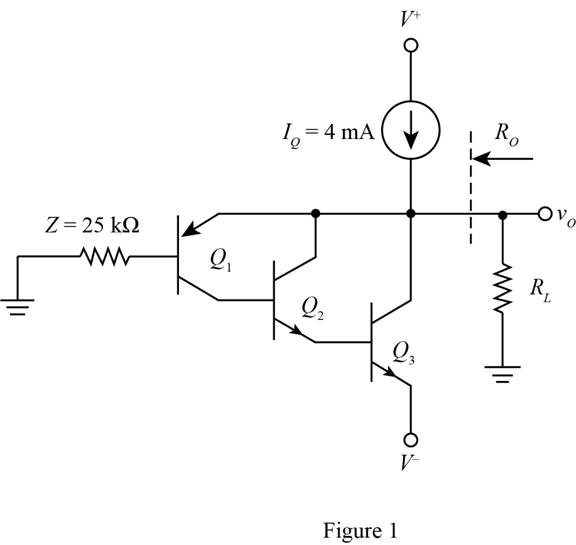
The expression for the value of base current of transistor
The expression for the value of the collector current for transitory
The expression for the value of the base current for transistor
The expression for the value of the base current for the transistor
The expression for the value of
The expression for the value of the collector current through the transistor
The expression for the value of the collector current for the transistor
The expression for the value of the collector current for transistor
The conversion from
The conversion from
The expression for the value of the quiescent current is given by,
Substitute
Substitute
The expression for the value of the collector current
Substitute
Substitute
Substitute
The expression for the value of
The expression for the value of
The expression for the value of
Substitute
Substitute
The expression for the value of
Substitute
The expression for the value of current
Substitute
The expression to determine the value of
Substitute
Substitute
Conclusion:
Therefore, the value of output resistance is
Want to see more full solutions like this?
Chapter 8 Solutions
Microelectronics: Circuit Analysis and Design


- (a) A current source with Rout = βoro is used to bias a standard bipolar differential amplifier. What is an expression for the CMRR of this amplifier for single-ended outputs?arrow_forwardDesign a feasible class A silicon BJT Power Amplifier that provides a high voltagegain using 15 volts supply and employs a concept to increase its loaded efficiency to50% so that little power loss is provided at the collector terminal.Given by manufacturer for safe operation, the amplifying component has a DCcurrent gain of 200 and a collector current limit of 4mA. The output stage of theAmplifier drives a headphone with 32-ohms load impedance applicable forsmartphones.arrow_forwardThe ac equivalent circuit for an amplifier is shown . Assume the capacitors have infinite value, RI = 750 Ω, RB = 100 kΩ, RC = 62 kΩ, and R3 = 100 kΩ. Calculate the voltage gain and input resistance for the amplifier if the BJT Q-point is (40μA, 10 V). Assume βo = 100 and VA = 75V.arrow_forward
- The bipolar differential amplifier as shown is biased by a 75-μA current source with an output resistance of 1MΩ. If the transistors have Early voltages of 60 V, estimate values of Rod, Roc, idm, and icm.arrow_forwardb. Design a feasible class A silicon BJT Power Amplifier that provides a high voltagegain using 15 volts supply and employs a concept to increase its loaded efficiency to50% so that little power loss is provided at the collector terminal.Given by manufacturer for safe operation, the amplifying component has a DCcurrent gain of 200 and a collector current limit of 4mA. The output stage of theAmplifier drives a headphone with 32-ohms load impedance applicable forsmartphones.arrow_forwardFor the follower circuit, let transistor Q1 have β = 50 and transistor Q2 have β = 100, and neglect the effect for ro. Use VBE = 0,7V. (a) Find the dc emitter currents of Q1 and Q2. Also, find the dc voltages VB1 and VB2. (b) If a load resistance RL = 1 kΩ is connected to the output terminal, find the voltage gain from the base to the emitter of Q2, , vo/vb2, and find the input resistance Rib2 looking into the base of Q2. (Hint: Consider Q2 as an emitter follower fed by a voltage Vb2 at its base). (c) Replacing Q2 with its input resistance Rib2 found in (b), analyze the circuit of emitter follower Q1 to determine its input resistance Rin, and the gain from its base to its emitter, ve1/vb1arrow_forward
- How does BJT Biasing Circuit works? Explain the working principle of BJT Biasing CircuitIf you can answer it within 1 hour I will upvote.arrow_forwardRefer to the differential amplifier circuit shown below . Determine the quiescent DC voltage at the collector terminal of each transistor assuming VBE of two transistor are negligible. What will be the quiescent DC values if VBE is taken to be 0.7 V.arrow_forwardDesign a Single-Stage Common Emitter Class A Amplifier Specifications:Voltage Divider Bias Circuit Supply: Any value from 10Vdc to 24VdcLoad: 1kΩVoltage Gain: Any value from 80 to 400Lower Cutoff Frequency: 100 HzSinusoidal source (zero internal resistance): 50mVp-pTransistor: Si, β = 75 • Base-Collector capacitance = 8pF • Base-Emitter Capacitance = 25pF a) compute for the biasing resistances.b) determine the dc transistor terminal voltages and transistor currents.arrow_forward
- The figure below shows the small-signal, equivalent-circuit model of a bipolar junction transistor (BJT). With rx = 180 Ω, rπ = 2.9 kΩ, rμ = 14 MΩ, ro = 140 kΩ, and gm = 80 mA/V. Calculate the values of its g-parameters.arrow_forwardThe ac equivalent circuit for an amplifier is shown. Assume the capacitors have infinite value, RI =750Ω, RB =100 kΩ, RC =100 kΩ, and R3 =100 kΩ. Calculate the input resistance and output resistance for the amplifier if the BJT Q-point is (75 μA, 10 V). Assume βo =100 and VA =75 V.arrow_forwardConsider the common-source amplifier shown in Figure P11.50. The NMOS transistor has KP=50 μA/V2, L=5 μm, W=500 μm, Vto=1 V and rd=∞.a. Determine the values of IDQ, VDSQ and gm. b. Compute the voltage gain, input resistance, and output resistance, assuming that the coupling capacitors are short circuits for the ac signal. Repeat Problem P11.50 for an NMOS transistor having KP=50 μA/V2, W=600 μm, L=20 μm, Vto=2 V and rd=∞. Compare the gain with that attained in Problem P11.50.arrow_forward
 Introductory Circuit Analysis (13th Edition)Electrical EngineeringISBN:9780133923605Author:Robert L. BoylestadPublisher:PEARSON
 Delmar's Standard Textbook Of ElectricityElectrical EngineeringISBN:9781337900348Author:Stephen L. HermanPublisher:Cengage Learning
 Programmable Logic ControllersElectrical EngineeringISBN:9780073373843Author:Frank D. PetruzellaPublisher:McGraw-Hill Education
 Fundamentals of Electric CircuitsElectrical EngineeringISBN:9780078028229Author:Charles K Alexander, Matthew SadikuPublisher:McGraw-Hill Education
 Electric Circuits. (11th Edition)Electrical EngineeringISBN:9780134746968Author:James W. Nilsson, Susan RiedelPublisher:PEARSON
 Engineering ElectromagneticsElectrical EngineeringISBN:9780078028151Author:Hayt, William H. (william Hart), Jr, BUCK, John A.Publisher:Mcgraw-hill Education,