
Videos
For the class−AB output stage in Figure 8.36, the parameters are:
(a)
The value of
Answer to Problem 8.49P
The value of the
Explanation of Solution
Calculation:
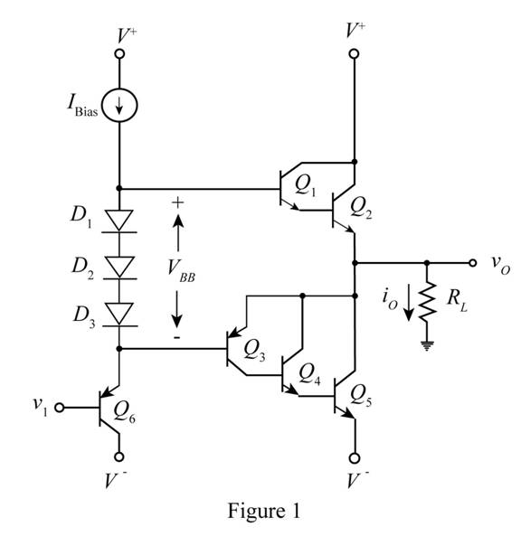
The given diagram is shown in Figure 1
The conversion from
The conversion from
The expression for the value of voltage
Substitute
The expression for the value of the voltage
The expression for the value of the voltage
The expression for the value of the voltage
The expression for the value of
The expression for the value of
The expression for the value of the voltage
Substitute
Substitute
Substitute
Substitute
Substitute
Substitute
Substitute
Substitute
Substitute
Conclusion:
Therefore, the value of the current
(b)
The value of the quiescent collector current in each transistor and the value of the collector quiescent current and the instantaneous power dissipated in
Answer to Problem 8.49P
The is
Explanation of Solution
Calculation:
The expression for the value of maximum output voltage is given by,
Substitute
The expression for the value of the current delivered to the load is given by,
Substitute
Apply KCL at the output node.
Substitute
The expression for the value of the current
Substitute
The expression for the value of the current
Substitute
The expression for the value of the voltage
Substitute
The expression for the value of the current
Substitute
The expression for the value of the current
Substitute
The expression for the value of power dissipated in the transistor
Substitute
The expression for the value of power dissipated in the transistor
Substitute
Conclusion:
Therefore, the value of the current
Want to see more full solutions like this?
Chapter 8 Solutions
Microelectronics: Circuit Analysis and Design


- The ac equivalent circuit for an amplifier is shown. Assume the capacitors have infinite value, RI = 100 kΩ, RG = 6.8MΩ, RD = 50 kΩ, and R3 = 120 kΩ. Calculate the voltage gain for the amplifier if the MOSFET Q-point is (100 μA, 5 V). Assume Kn = 450 μA/V2 and λ = 0.02 V−1.arrow_forwardDesign a VCO circuit that will produce a square wave output at 2.6 kHz.arrow_forwardSince IDSS=8 mA, VGS(off) = -10V according to the circuit on the side, if the capacitor C2 is removed, what will be the Av gain value?arrow_forward
- For the circuit given below, let VBEQ=0.7 V, then the Q-point(VCEQ,ICEQ) equals:arrow_forwardDesign a Single-Stage Common Emitter Class A Amplifier Specifications:Voltage Divider Bias Circuit Supply: Any value from 10Vdc to 24VdcLoad: 1kΩVoltage Gain: Any value from 80 to 400Lower Cutoff Frequency: 100 HzSinusoidal source (zero internal resistance): 50mVp-pTransistor: Si, β = 75 • Base-Collector capacitance = 8pF • Base-Emitter Capacitance = 25pF a) compute for the biasing resistances.b) determine the dc transistor terminal voltages and transistor currents.arrow_forwardIn the circuit in the figure, VGSQ = 6.8 V, IDQ = 2.4 mA, VGS(Th) = 3.3 V, k = 0.4x10⁻³ A/V2, RD = 5.6 kΩ, RF = 2.2 MΩ and rd = 25 kΩ. Accordingly, when a RL = 0.1 kΩ load is connected to the output of the circuit, what will be the voltage gain of the circuit? NOTE: MOSFET output resistance must be taken into account in rd calculationsarrow_forward
- The outer surface of a transistor is cooled convectively by a fan-induced flow of air ata temperature of 25 °C and a pressure of 1 atm. The transistor’s outer surface area is 5x 10 -4 m 2 . At steady state, the electrical power to the transistor is 3 W. Negligible heattransfer occurs through the base of the transistor. The convective heat transfercoefficient is 100 W/m 2 K.Determinei. the rate of heat transferbetween the transistor and theair, in Wii. the temperature at thetransistor’s outer surface, in °C.arrow_forwardSubject : ELECTRONIC CIRCUIT ANALYSIS AND DEVICES Please give the DC ANALYSIS circuit and AC EQUIVALENT CIRCUIT of this problem before proceeding to find letters a, and b. (Note : Neglect Vbe)arrow_forwardThe ac equivalent circuit for an amplifier is shown . Assume the capacitors have infinite value, RI = 750 Ω, RB = 100 kΩ, RC = 62 kΩ, and R3 = 100 kΩ. Calculate the voltage gain and input resistance for the amplifier if the BJT Q-point is (40μA, 10 V). Assume βo = 100 and VA = 75V.arrow_forward
- The ac equivalent circuit for an amplifier is shown. Assume the capacitors have infinite value, RI =750Ω, RB =100 kΩ, RC =100 kΩ, and R3 =100 kΩ. Calculate the input resistance and output resistance for the amplifier if the BJT Q-point is (75 μA, 10 V). Assume βo =100 and VA =75 V.arrow_forwardIn the Mosfet circuit given below, R1+R2=50 kΩ, RD= 7.5 kΩ, VDD= 5V, VTP= -0.8 V, Kp= 0.2 mA/V2 is given. Calculate the ID current by determining the working region of the mosfet.arrow_forwardA Hartley Oscillator circuit having two individual inductors of 0.5mH each, are designed toresonate in parallel with a variable capacitor that can be adjusted between 100pF and 500pF.Determine the upper and lower frequencies of oscillation and also the Hartley oscillatorsbandwidth.arrow_forward
 Introductory Circuit Analysis (13th Edition)Electrical EngineeringISBN:9780133923605Author:Robert L. BoylestadPublisher:PEARSON
 Delmar's Standard Textbook Of ElectricityElectrical EngineeringISBN:9781337900348Author:Stephen L. HermanPublisher:Cengage Learning
 Programmable Logic ControllersElectrical EngineeringISBN:9780073373843Author:Frank D. PetruzellaPublisher:McGraw-Hill Education
 Fundamentals of Electric CircuitsElectrical EngineeringISBN:9780078028229Author:Charles K Alexander, Matthew SadikuPublisher:McGraw-Hill Education
 Electric Circuits. (11th Edition)Electrical EngineeringISBN:9780134746968Author:James W. Nilsson, Susan RiedelPublisher:PEARSON
 Engineering ElectromagneticsElectrical EngineeringISBN:9780078028151Author:Hayt, William H. (william Hart), Jr, BUCK, John A.Publisher:Mcgraw-hill Education,