Microelectronics: Circuit Analysis and Design
4th Edition
ISBN: 9780073380643
Author: Donald A. Neamen
Publisher: McGraw-Hill Companies, The
bartleby

Concept explainers

bartleby

Videos

Textbook Question
Book Icon
Chapter 9, Problem 9.67P

Assume the instrumentation amplifier in Figure 9.26 has ideal op-amps. Thecircuit parameters are R 1 = 10 k Ω , R 2 = 40 k Ω , R 3 = 40 k Ω , and R 4 = 120 k Ω . Determine v O 1 , v O 2 , v O , and the current in R 1 for(a) v I 2 = 1.2 + 0.08 sin ω t ( V ) , v I 1 = 1.2 0.08 sin ω t ( V ) ; and (b v I 2 = 0.60 0.05 sin ω t ( V ) , v I 1 = 0.65 + 0.05 sin ω t ( V )

(a)

Expert Solution
Check Mark
To determine

The values of the voltages vO1 , vO2 and vO .

Also, the current through the resistance R1 .

Answer to Problem 9.67P

The expression for the voltage vO2 is 1.2+0.72sinωtV , voltage vO1 is 1.2+0.72sinωtV , vO is 4.32sinωtV and the value of the current through the resistance R1 is 16×103sinωtA .

Explanation of Solution

Calculation:

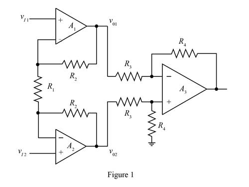
The given diagram is shown in Figure 1

  Microelectronics: Circuit Analysis and Design, Chapter 9, Problem 9.67P , additional homework tip  1

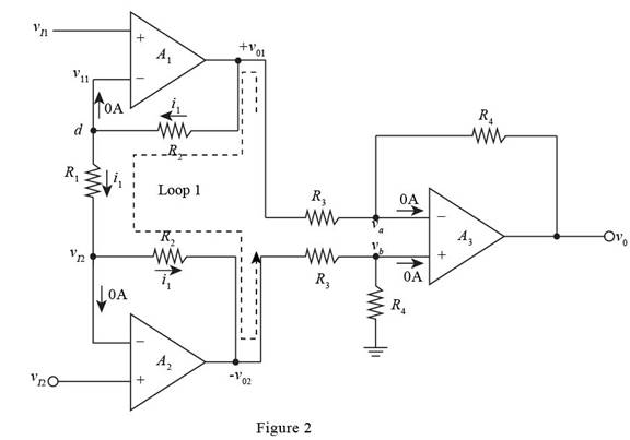
Mark the voltages and current and redraw the circuit.

The required diagram is shown in Figure 2

  Microelectronics: Circuit Analysis and Design, Chapter 9, Problem 9.67P , additional homework tip  2

The expression for the voltage vb by voltage division rule is given by,

  vb=R4vO2R3+R4

The expression for the current at the node va is given by,

  va=vb

Substitute R4vO2R3+R4 for vb in the above equation.

  va=R4vO2R3+R4

Apply KCL at the node va .

  v O1vaR3=vavOR4R4R3vO1va[ R 4+ R 3 R 3]=vO

Substitute vb for va in the above equation.

  R4R3vO1vb[R4+R3R3]=vO

Substitute R4vO2R3+R4 for vb in the above equation.

  R4R3vO1( R 4 v O2 R 3 + R 4 )[ R 4+ R 3 R 3]=vOvO=R4R3(v O2v O1) …… (1)

The expression for the current i1 is given by,

  i1=vI1vI2R1 …… (2)

Apply KVL in the loop 1

  vO1vO2=i1R2+i1R1+i1R2=i1(R1+2R2)

Substitute vI1vI2R1 for i1 in the above equation.

  vO1vO2=(v I2v I1R1)(R1+2R2)

Substitute (v I2v I1R1)(R1+2R2) for vO1vO2 in equation (1).

  vO=R4R3(v I2v I1R1)(R1+2R2)

Substitute 10kΩ for R1 , 40kΩ for R2 , 40kΩ for R3 and 120kΩ for R4 in the above equation.

  vO=120kΩ( 40kΩ)( v I2 v I1 10kΩ)(10kΩ+2( 40kΩ))=27(v I2v I1) …… (3)

Substitute 1.2+0.08sinωtV for vI1 and 1.20.08sinωtV for vI2 in the above equation.

  vO=27(1.2+0.08sinωtV1.2+0.08sinωtV)=4.32sinωtV

Substitute 10kΩ for R1 , 1.2+0.08sinωtV for vI1 and 1.20.08sinωtV for vI2 in equation (2).

  i1=1.20.08sinωtV( 1.2+0.08sinωtV)10kΩ=16×103sinωtmA

The expression for the current i1 is given by,

  i1=v O1v I1R2vO1=i1R2+vI1 …… (4)

Substitute 0.08sinωt for vI1 , 16×103sinωtmA for i1 , 40kΩ for R2 in the above equation.

  vO1=(16× 10 3sinωtmA)(40kΩ)0.08sinωt=1.20.72sinωtV

The expression for the voltage vO2 is given by,

  vO2=vI2i1R2 …… (5)

Substitute 0.08sinωt for vI2 , 16×103sinωtmA for i1 , 40kΩ for R2 in the above equation.

  vO2=1.2+0.08sinωt(16× 10 3sinωtmA)(40kΩ)=1.2+0.72sinωtV

Conclusion:

Therefore, theexpression for the voltage vO2 is 1.2+0.72sinωtV , voltage vO1 is 1.2+0.72sinωtV , vO is 4.32sinωtV and the value of the current through the resistance R1 is 16×103sinωtA .

(b)

Expert Solution
Check Mark
To determine

The values of the voltages vO1 , vO2 and vO .

Also the current through the resistance R1 .

Answer to Problem 9.67P

The expression for the voltage vO2 is 0.40.45sinωtV , voltage vO1 is 0.85+0.45inωtV , vO is 1.352.7sinωtV and the value of the current through the resistance R1 is (5+10)103sinωtmA .

Explanation of Solution

Calculation:

Substitute 0.600.05sinωtV for vI2 and 0.65+0.05sinωtV for vI1 equation (3).

  vO=27(0.600.05sinωtV0.60+0.05sinωtV)=1.352.7sinωtV

Substitute 10kΩ for R1 , 0.65+0.05sinωtV for vI1 and 0.600.06sinωtV for vI2 in equation (2).

  i1=0.65+0.05sinωtV( 0.600.06sinωtV)10kΩ=(5+10)103sinωtmA

Substitute 0.65+0.05sinωtV for vI1 , (5+10)103sinωtmA for i1 , 40kΩ for R2 in the above equation.

  vO1=(( 5+10) 10 3sinωtmA)(40kΩ)0.65+0.05sinωtV=0.85+0.45inωtV

Substitute 0.600.05sinωtV for vI2 , (5+10)103sinωtmA for i1 , 40kΩ for R2 equation (5)

  vO2=0.600.05sinωtV(( 5+10) 10 3sinωtmA)(40kΩ)=0.40.45sinωtV

Conclusion:

Therefore, the expression for the voltage vO2 is 0.40.45sinωtV , voltage vO1 is 0.85+0.45inωtV , vO is 1.352.7sinωtV and the value of the current through the resistance R1 is (5+10)103sinωtmA .

Want to see more full solutions like this?

Subscribe now to access step-by-step solutions to millions of textbook problems written by subject matter experts!
Students have asked these similar questions
The op amp circuit shown is ideal.  The values for the circuit are as follows:+VCC = 12.0V, -VCC = -10.0V, Ra = 9.00Ω, Rb = 30.0Ω, Rc = 42.0Ω, Rd = 4.00Ω, Re = 32.0Ω. Write a KCL equation at node n. Solve for the output voltage vout as a function of the inputs va and vb. If input va=2.00V and output vout =10.0V, then solve for input vb. If inputs va=8.00V and vb=5.00V, then solve for the power absorbed by Rb. If input va=4.00V, then solve for the range of input vb such that the amplifier does not saturate.
A. Give 3 possible problems rn that can relate on electrical engineering and give a solution that can aware public.
The op amp circuit shown is ideal.  The values for the circuit are as follows:+VCC = 12.0V, -VCC = -10.0V, Ra = 30.0Ω, Rb = 70.0Ω, Rc = 2.00Ω, Rd = 5.00Ω, Re = 12.0Ω, Rf = 4.00Ω. Write a KCL equation at node n. Solve for the output voltage vout as a function of the inputs va and vb. If input vb= -2.00V and output vout =10.0V, then solve for input va. If inputs va=8.00V and vb=9.00V, then solve for the power absorbed by Ra. If input va=6.00V, then solve for the range of input vb such that the amplifier does not saturate.

Chapter 9 Solutions

Microelectronics: Circuit Analysis and Design

Ch. 9 - The noninverting op-amp in Figure 9.15 has a...Ch. 9 - Use superposition to determine the output voltage...Ch. 9 - Consider the voltage-to-current converter shown in...Ch. 9 - Consider the difference amplifier in Figure...Ch. 9 - In the difference amplifier shown in Figure...Ch. 9 - For the instrumentation amplifier in Figure 9.26,...Ch. 9 - An integrator with input and output voltages that...Ch. 9 - A current source has an output impedance of...Ch. 9 - Design the voltage-to-current converter shown in...Ch. 9 - All parameters associated with the instrumentation...Ch. 9 - Design the instrumentation amplifier in Figure...Ch. 9 - An integrator is driven by the series of pulses...Ch. 9 - Consider the summing op-amp in Figure 9.40. Let...Ch. 9 - Consider the bridge circuit in Figure 9.46. The...Ch. 9 - The resistance R in the bridge circuit in Figure...Ch. 9 - Describe the ideal op-amp model and describe the...Ch. 9 - Prob. 2RQCh. 9 - Describe the operation and characteristics of the...Ch. 9 - What is the concept of virtual ground?Ch. 9 - What is the significance of a zero output...Ch. 9 - When a finite op-amp gain is taken into account,...Ch. 9 - Prob. 7RQCh. 9 - Describe the operation and characteristics of the...Ch. 9 - Describe the voltage follower. What are the...Ch. 9 - What is the input resistance of an ideal...Ch. 9 - Prob. 11RQCh. 9 - Describe the operation and characteristics of an...Ch. 9 - Describe the operation and characteristics of an...Ch. 9 - Describe the operation and characteristics of an...Ch. 9 - Assume an op-amp is ideal, except for having a...Ch. 9 - The op-amp in the circuit shown in Figure P9.2 is...Ch. 9 - An op-amp is in an open-loop configuration as...Ch. 9 - Consider the equivalent circuit of the op-amp...Ch. 9 - Consider the ideal inverting op-amp circuit shown...Ch. 9 - Assume the op-amps in Figure P9.6 are ideal. Find...Ch. 9 - Consider an ideal inverting op-amp with R2=100k...Ch. 9 - (a) Design an inverting op-amp circuit with a...Ch. 9 - Consider an ideal op-amp used in an inverting...Ch. 9 - Consider the inverting amplifier shown in Figure...Ch. 9 - (a) Design an inverting op-amp circuit with a...Ch. 9 - (a) Design an inverting op-amp circuit such that...Ch. 9 - (a) In an inverting op-amp circuit, the nominal...Ch. 9 - (a) The input to the circuit shown in Figure P9.14...Ch. 9 - Design an inverting amplifier to provide a nominal...Ch. 9 - The parameters of the two inverting op-amp...Ch. 9 - Design the cascade inverting op-amp circuit in...Ch. 9 - Design an amplifier system with three inverting...Ch. 9 - Consider the circuit shown in Figure P9.19. (a)...Ch. 9 - The inverting op-amp shown in Figure 9.9 has...Ch. 9 - (a)An op-amp with an open-loop gain of Aod=7103 is...Ch. 9 - (a) For the ideal inverting op-amp circuit with...Ch. 9 - An ideal inverting op-amp circuit is to be...Ch. 9 - For the op-amp circuit shown in Figure P9.25,...Ch. 9 - The inverting op-amp circuit in Figure 9.9 has...Ch. 9 - (a) Consider the op-amp circuit in Figure P9.27....Ch. 9 - The circuit in Figure P9.28 is similar to the...Ch. 9 - Consider the ideal inverting summing amplifier in...Ch. 9 - (a) Design an ideal inverting summing amplifier to...Ch. 9 - Design an ideal inverting summing amplifier to...Ch. 9 - Consider the summing amplifier in Figure 9.14 with...Ch. 9 - The parameters for the summing amplifier in Figure...Ch. 9 - (a) Design an ideal summing op-amp circuit to...Ch. 9 - An ideal three-input inverting summing amplifier...Ch. 9 - A summing amplifier can be used as a...Ch. 9 - Consider the circuit in Figure P9.38. (a) Derive...Ch. 9 - Consider the summing amplifier in Figure 9.14(a)....Ch. 9 - Consider the ideal noninverting op-amp circuit in...Ch. 9 - (a) Design an ideal noninverting op-amp circuit...Ch. 9 - Consider the noninverting amplifier in Figure...Ch. 9 - For the circuit in Figure P9.43, the input voltage...Ch. 9 - Determine vO as a function of vI1 and vI2 for the...Ch. 9 - Consider the ideal noninverting op-amp circuit in...Ch. 9 - (a) Derive the expression for the closed-loop...Ch. 9 - The circuit shown in Figure P9.47 can be used as a...Ch. 9 - (a) Determine the closed-loop voltage gain...Ch. 9 - For the amplifier in Figure P9.49, determine (a)...Ch. 9 - Consider the voltage-follower circuit in Figure...Ch. 9 - (a) Consider the ideal op-amp circuit shown in...Ch. 9 - (a) Assume the op-amp in the circuit in Figure...Ch. 9 - Prob. 9.53PCh. 9 - A current-to-voltage converter is shown in Figure...Ch. 9 - Figure P9.55 shows a phototransistor that converts...Ch. 9 - The circuit in Figure P9.56 is an analog voltmeter...Ch. 9 - Consider the voltage-to-current converter in...Ch. 9 - The circuit in Figure P9.58 is used to drive an...Ch. 9 - Figure P9.59 is used to calculate the resistance...Ch. 9 - Consider the op-amp difference amplifier in Figure...Ch. 9 - Consider the differential amplifier shown in...Ch. 9 - Consider the differential amplifier shown in...Ch. 9 - Let R=10k in the differential amplifier in Figure...Ch. 9 - Consider the circuit shown in Figure P9.64. (a)...Ch. 9 - The circuit in Figure P9.65 is a representation of...Ch. 9 - Consider the adjustable gain difference amplifier...Ch. 9 - Assume the instrumentation amplifier in Figure...Ch. 9 - Consider the circuit in Figure P9.68. Assume ideal...Ch. 9 - Consider the circuit in Figure P969. Assume ideal...Ch. 9 - The instrumentation amplifier in Figure 9.26 has...Ch. 9 - Design the instrumentation amplifier in Figure...Ch. 9 - All parameters associated with the instrumentation...Ch. 9 - The parameters in the integrator circuit shown in...Ch. 9 - Consider the ideal op-amp integrator. Assume the...Ch. 9 - The circuit in Figure P9.75 is a first-order...Ch. 9 - (a) Using the results of Problem 9.75, design the...Ch. 9 - The circuit shown in Figure P9.77 is a first-order...Ch. 9 - (a) Using the results of Problem 9.77, design the...Ch. 9 - Prob. 9.79PCh. 9 - Consider the circuit in Figure 9.35. The diode...Ch. 9 - In the circuit in Figure P9.81, assume that Q1 and...Ch. 9 - Consider the circuit in Figure 9.36. The diode...Ch. 9 - Design an op-amp summer to produce the output...Ch. 9 - Design an op-amp summer to produce an output...Ch. 9 - Design a voltage reference source as shown in...Ch. 9 - Consider the voltage reference circuit in Figure...Ch. 9 - Consider the bridge circuit in Figure P9.87. The...Ch. 9 - Consider the bridge circuit in Figure 9.46. The...
Knowledge Booster
Background pattern image
Electrical Engineering
Learn more about
Need a deep-dive on the concept behind this application? Look no further. Learn more about this topic, electrical-engineering and related others by exploring similar questions and additional content below.
Similar questions
SEE MORE QUESTIONS
Recommended textbooks for you
Text book image
Introductory Circuit Analysis (13th Edition)
Electrical Engineering
ISBN:9780133923605
Author:Robert L. Boylestad
Publisher:PEARSON
Text book image
Delmar's Standard Textbook Of Electricity
Electrical Engineering
ISBN:9781337900348
Author:Stephen L. Herman
Publisher:Cengage Learning
Text book image
Programmable Logic Controllers
Electrical Engineering
ISBN:9780073373843
Author:Frank D. Petruzella
Publisher:McGraw-Hill Education
Text book image
Fundamentals of Electric Circuits
Electrical Engineering
ISBN:9780078028229
Author:Charles K Alexander, Matthew Sadiku
Publisher:McGraw-Hill Education
Text book image
Electric Circuits. (11th Edition)
Electrical Engineering
ISBN:9780134746968
Author:James W. Nilsson, Susan Riedel
Publisher:PEARSON
Text book image
Engineering Electromagnetics
Electrical Engineering
ISBN:9780078028151
Author:Hayt, William H. (william Hart), Jr, BUCK, John A.
Publisher:Mcgraw-hill Education,
Multistage Transistor Audio Amplifier Circuit; Author: The Organic Chemistry Tutor;https://www.youtube.com/watch?v=LJrL9N9uhkE;License: Standard Youtube License