
Concept explainers
Videos
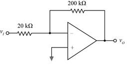
Assume the op-amps in Figure P9.6 are ideal. Find the voltage gain
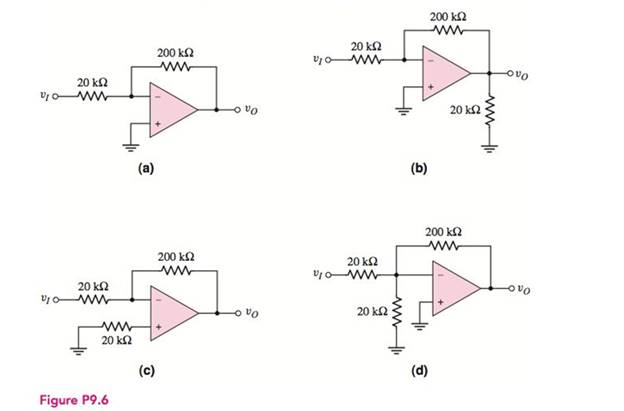
(a)
The voltage gain
Answer to Problem 9.6P
The value of the voltage gain is
Explanation of Solution
Calculation:
The given diagram is shown in Figure 1
Mark the values and redraw the circuit of part (a).
The required diagram is shown in Figure 2
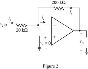
The from the above circuit the expression for the value of the voltage
Substitute
The value of the current
The expression for the value of the voltage gain is given by,
Apply KCL at the negative terminal.
Substitute
The expression for the value of the current
Substitute
Substitute
Substitute
The expression for the value of the input resistance is given by,
Substitute
Conclusion:
Therefore, the value of the voltage gain is
(b)
The voltage gain
Answer to Problem 9.6P
The value of the voltage gain is
Explanation of Solution
Calculation:
Mark the values and redraw the circuit of part (b).
The required diagram is shown in Figure 3
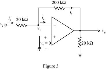
The from the above circuit the expression for the value of the voltage
Substitute
The value of the current
The expression for the value of the voltage gain is given by,
Apply KCL at the negative terminal.
Substitute
The expression for the value of the current
Substitute
Substitute
Substitute
The expression for the value of the input resistance is given by,
Substitute
Conclusion:
Therefore, the value of the voltage gain is
(c)
The voltage gain
Answer to Problem 9.6P
The value of the voltage gain is
Explanation of Solution
Calculation:
Mark the values and redraw the circuit of part (c).
The required diagram is shown in Figure 4
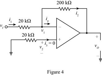
The from the above circuit the expression for the value of the voltage
Substitute
The value of the current
The expression for the value of the voltage gain is given by,
Apply KCL at the negative terminal.
Substitute
The expression for the value of the current
Substitute
Substitute
Substitute
The expression for the value of the input resistance is given by,
Substitute
Conclusion:
Therefore, the value of the voltage gain is
(d)
The voltage gain
Answer to Problem 9.6P
The value of the voltage gain is
Explanation of Solution
Calculation:
Mark the values and redraw the circuit of part (d).
The required diagram is shown in Figure 5
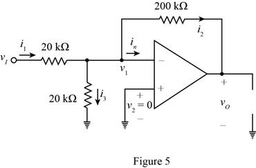
The from the above circuit the expression for the value of the voltage
Substitute
The value of the current
The expression for the value of the voltage gain is given by,
Apply KCL at the negative terminal.
Substitute
The expression for the value of the current is given by,
Apply KVL at the inverting terminal.
Substitute
Substitute
Substitute
The expression for the value of the input resistance is given by,
Substitute
Conclusion:
Therefore, thevalue of the voltage gain is
Want to see more full solutions like this?
Chapter 9 Solutions
Microelectronics: Circuit Analysis and Design


- Determine the output voltage of the ideal op-amp differentiator in Figure below for the triangular-wave input shown.arrow_forwardDetermine the closed-loop voltage gain of the circuit shown in the figure assumingan ideal op amparrow_forwardWhich op-amp will produce an outputthat is more similar to the output of an ideal op-amp?arrow_forward
- III Determine the output voltage of the ideal op - amp differentiator in Figure below for the triangular - wave input shown.arrow_forwardSuppose that we are designing an amplifier, using an op amp. What problems are associated with using very small feedback resistances? With very large feedback resistances?arrow_forwardExplain with the help of proper diagram and necessary derivation, How Op-Amp can be used as inverting , noninverting and difference amplifier. Assume open loop configuration.arrow_forward
 Introductory Circuit Analysis (13th Edition)Electrical EngineeringISBN:9780133923605Author:Robert L. BoylestadPublisher:PEARSON
 Delmar's Standard Textbook Of ElectricityElectrical EngineeringISBN:9781337900348Author:Stephen L. HermanPublisher:Cengage Learning
 Programmable Logic ControllersElectrical EngineeringISBN:9780073373843Author:Frank D. PetruzellaPublisher:McGraw-Hill Education
 Fundamentals of Electric CircuitsElectrical EngineeringISBN:9780078028229Author:Charles K Alexander, Matthew SadikuPublisher:McGraw-Hill Education
 Electric Circuits. (11th Edition)Electrical EngineeringISBN:9780134746968Author:James W. Nilsson, Susan RiedelPublisher:PEARSON
 Engineering ElectromagneticsElectrical EngineeringISBN:9780078028151Author:Hayt, William H. (william Hart), Jr, BUCK, John A.Publisher:Mcgraw-hill Education,