Microelectronics: Circuit Analysis and Design
4th Edition
ISBN: 9780073380643
Author: Donald A. Neamen
Publisher: McGraw-Hill Companies, The
bartleby

Videos

Textbook Question
Book Icon
Chapter 9, Problem 9.72P

All parameters associated with the instrumentation amplifier in Figure 9.26are the same as given in Exercise Ex 9.8, except that resistor R 3 , which isconnected to the inverting terminal of A3, is R 3 = 30 k Ω ± 5 % . Determinethe maximum common-mode gain.

Expert Solution & Answer
Check Mark
To determine

The value of maximum common mode gain.

Answer to Problem 9.72P

The maximum value of the voltage gain is 0.0395 .

Explanation of Solution

Calculation:

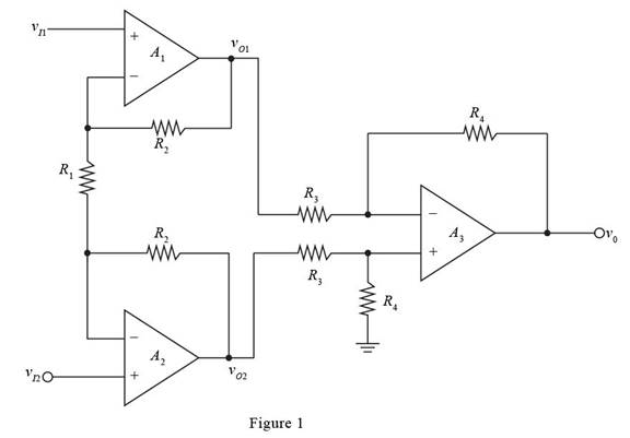
The given diagram is shown in Figure 1

  Microelectronics: Circuit Analysis and Design, Chapter 9, Problem 9.72P , additional homework tip  1

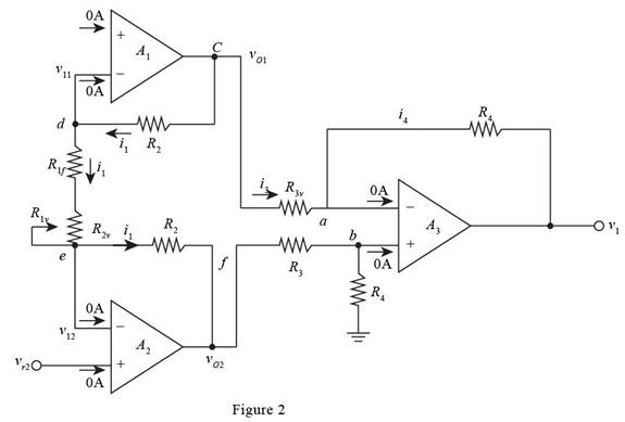
Mark the voltages and current and redraw the circuit.

The required diagram is shown in Figure 2

  Microelectronics: Circuit Analysis and Design, Chapter 9, Problem 9.72P , additional homework tip  2

The expression for the voltage vb by voltage division rule is given by,

  vb=R4vO2R3+R4

The expression for the current at the node va is given by,

  va=vb

Substitute R4vO2R3+R4 for vb in the above equation.

  va=R4vO2R3+R4

Apply KCL at the node va .

  v O1vaR 3x=vavOR4vO=( R 4 R 3x )vO1+(1+ R 4 R 3x )va

Substitute R4vO2R3+R4 for va in the above equation.

  vO=(R4R 3x)vO1+(1+R4R 3x)R4vO2R3+R4 ........ (1)

The expression for the value of the current i1 is given by,

  i1=vI1vI2R1

The expression for the voltage vO1 is given by,

  vO1vI1=i1R2

Substitute vI1vI2R1 for i1 in the above equation.

  vO1=vI1+(v I1v I2R1)R2

The expression for the voltage vO2 is given by,

  vO2=vI2i1R2

Substitute vI1vI2R1 for i1 in the above equation.

  vO2=vI2(v I1v I2R1)R2

Substitute vI1+(v I1v I2R1)R2 for vO1 and vI2(v I1v I2R1)R2 for vO2 in equation (1)

  vO=( R 4 R 3x )(v I1+( v I1 v I2 R 1 )R2)+(1+ R 4 R 3x )R4R3+R4(v I2( v I1 v I2 R 1 )R2)=( v I1 v I2 R 1 )R2[( R 4 R 3x )(1+ R 4 R 3x )(1+ R 4 R 3 + R 4 )]vI1( R 4 R 3x )+vI2(1+ R 4 R 3x )( R 4 R 3 + R 4 ) ........ (2)

The expression for the common mode voltage is given by,

  vcm=vI1+vI22

The expression for the differential voltage is given by,

  vd=vI2vI1

The expression for the voltage vI2 is given by,

  vI2=vcm+vd2

The expression for the voltage vI1 is given by,

  vI1=vcmvd2

Substitute vd for vI2vI1 , vcm+vd2 for vI2 and vcmvd2 for vI1 in equation (2).

  vO=[( v d R 1 ) R 2[ ( R 4 R 3x )( 1+ R 4 R 3x )( 1+ R 4 R 3 + R 4 )]( v cm v d 2 )( R 4 R 3x )+( v cm + v d 2 )( 1+ R 4 R 3x )( R 4 R 3 + R 4 )]=[ v d[ ( R 2 R 1 + 1 2 )( R 4 R 3x )( R 2 R 1 + 1 2 )( 1+ R 4 R 3x )( R 4 R 3 + R 4 )]+ v cm[ ( R 4 R 3x )+( 1+ R 4 R 3x )( R 4 R 3 + R 4 )]] ........ (3)

The general expression for the output equation is given by,

  vO=Acmvcm+Advd

From above and from equation (3), the expression for the common mode gain is evaluated as,

  Acm=(R4R 3x)+(1+R4R 3x)(R4R3+R4)

Substitute 90kΩ for R4 , 30kΩ for R3 and 30kΩ±5% for R3x in the above equation.

  Acm=( 90kΩ 30kΩ±5%)+(1+ 90kΩ 30kΩ±5%)( 90kΩ 30kΩ+90kΩ)=14[3( 90 30±5%)]

From above the range of the common mode voltage gain is given by,

  14[3( 90 305%)]Acm14[3( 90 30+5%)]0.0395Acm0.0357

The maximum value of the voltage gain is given by,

  |Acm|max=0.0395

Conclusion:

Therefore, themaximum value of the voltage gain is 0.0395 .

Want to see more full solutions like this?

Subscribe now to access step-by-step solutions to millions of textbook problems written by subject matter experts!
Students have asked these similar questions
What is the unity gain frequency and phase margin? (pls answer asap)
Identify an industrial application where MULTISTAGE AMPLIFIER is required and design circuit for the same application and Draw the appropriate circuit diagram, functioning diagram.
a) Sketch and explain the root locus curve. b) Calculate the separation point from the real axis and the gain here. c) Calculate the virtual axis cut-off points and also the gain values at this point. d) Determine and explain the stability range.

Chapter 9 Solutions

Microelectronics: Circuit Analysis and Design

Ch. 9 - The noninverting op-amp in Figure 9.15 has a...Ch. 9 - Use superposition to determine the output voltage...Ch. 9 - Consider the voltage-to-current converter shown in...Ch. 9 - Consider the difference amplifier in Figure...Ch. 9 - In the difference amplifier shown in Figure...Ch. 9 - For the instrumentation amplifier in Figure 9.26,...Ch. 9 - An integrator with input and output voltages that...Ch. 9 - A current source has an output impedance of...Ch. 9 - Design the voltage-to-current converter shown in...Ch. 9 - All parameters associated with the instrumentation...Ch. 9 - Design the instrumentation amplifier in Figure...Ch. 9 - An integrator is driven by the series of pulses...Ch. 9 - Consider the summing op-amp in Figure 9.40. Let...Ch. 9 - Consider the bridge circuit in Figure 9.46. The...Ch. 9 - The resistance R in the bridge circuit in Figure...Ch. 9 - Describe the ideal op-amp model and describe the...Ch. 9 - Prob. 2RQCh. 9 - Describe the operation and characteristics of the...Ch. 9 - What is the concept of virtual ground?Ch. 9 - What is the significance of a zero output...Ch. 9 - When a finite op-amp gain is taken into account,...Ch. 9 - Prob. 7RQCh. 9 - Describe the operation and characteristics of the...Ch. 9 - Describe the voltage follower. What are the...Ch. 9 - What is the input resistance of an ideal...Ch. 9 - Prob. 11RQCh. 9 - Describe the operation and characteristics of an...Ch. 9 - Describe the operation and characteristics of an...Ch. 9 - Describe the operation and characteristics of an...Ch. 9 - Assume an op-amp is ideal, except for having a...Ch. 9 - The op-amp in the circuit shown in Figure P9.2 is...Ch. 9 - An op-amp is in an open-loop configuration as...Ch. 9 - Consider the equivalent circuit of the op-amp...Ch. 9 - Consider the ideal inverting op-amp circuit shown...Ch. 9 - Assume the op-amps in Figure P9.6 are ideal. Find...Ch. 9 - Consider an ideal inverting op-amp with R2=100k...Ch. 9 - (a) Design an inverting op-amp circuit with a...Ch. 9 - Consider an ideal op-amp used in an inverting...Ch. 9 - Consider the inverting amplifier shown in Figure...Ch. 9 - (a) Design an inverting op-amp circuit with a...Ch. 9 - (a) Design an inverting op-amp circuit such that...Ch. 9 - (a) In an inverting op-amp circuit, the nominal...Ch. 9 - (a) The input to the circuit shown in Figure P9.14...Ch. 9 - Design an inverting amplifier to provide a nominal...Ch. 9 - The parameters of the two inverting op-amp...Ch. 9 - Design the cascade inverting op-amp circuit in...Ch. 9 - Design an amplifier system with three inverting...Ch. 9 - Consider the circuit shown in Figure P9.19. (a)...Ch. 9 - The inverting op-amp shown in Figure 9.9 has...Ch. 9 - (a)An op-amp with an open-loop gain of Aod=7103 is...Ch. 9 - (a) For the ideal inverting op-amp circuit with...Ch. 9 - An ideal inverting op-amp circuit is to be...Ch. 9 - For the op-amp circuit shown in Figure P9.25,...Ch. 9 - The inverting op-amp circuit in Figure 9.9 has...Ch. 9 - (a) Consider the op-amp circuit in Figure P9.27....Ch. 9 - The circuit in Figure P9.28 is similar to the...Ch. 9 - Consider the ideal inverting summing amplifier in...Ch. 9 - (a) Design an ideal inverting summing amplifier to...Ch. 9 - Design an ideal inverting summing amplifier to...Ch. 9 - Consider the summing amplifier in Figure 9.14 with...Ch. 9 - The parameters for the summing amplifier in Figure...Ch. 9 - (a) Design an ideal summing op-amp circuit to...Ch. 9 - An ideal three-input inverting summing amplifier...Ch. 9 - A summing amplifier can be used as a...Ch. 9 - Consider the circuit in Figure P9.38. (a) Derive...Ch. 9 - Consider the summing amplifier in Figure 9.14(a)....Ch. 9 - Consider the ideal noninverting op-amp circuit in...Ch. 9 - (a) Design an ideal noninverting op-amp circuit...Ch. 9 - Consider the noninverting amplifier in Figure...Ch. 9 - For the circuit in Figure P9.43, the input voltage...Ch. 9 - Determine vO as a function of vI1 and vI2 for the...Ch. 9 - Consider the ideal noninverting op-amp circuit in...Ch. 9 - (a) Derive the expression for the closed-loop...Ch. 9 - The circuit shown in Figure P9.47 can be used as a...Ch. 9 - (a) Determine the closed-loop voltage gain...Ch. 9 - For the amplifier in Figure P9.49, determine (a)...Ch. 9 - Consider the voltage-follower circuit in Figure...Ch. 9 - (a) Consider the ideal op-amp circuit shown in...Ch. 9 - (a) Assume the op-amp in the circuit in Figure...Ch. 9 - Prob. 9.53PCh. 9 - A current-to-voltage converter is shown in Figure...Ch. 9 - Figure P9.55 shows a phototransistor that converts...Ch. 9 - The circuit in Figure P9.56 is an analog voltmeter...Ch. 9 - Consider the voltage-to-current converter in...Ch. 9 - The circuit in Figure P9.58 is used to drive an...Ch. 9 - Figure P9.59 is used to calculate the resistance...Ch. 9 - Consider the op-amp difference amplifier in Figure...Ch. 9 - Consider the differential amplifier shown in...Ch. 9 - Consider the differential amplifier shown in...Ch. 9 - Let R=10k in the differential amplifier in Figure...Ch. 9 - Consider the circuit shown in Figure P9.64. (a)...Ch. 9 - The circuit in Figure P9.65 is a representation of...Ch. 9 - Consider the adjustable gain difference amplifier...Ch. 9 - Assume the instrumentation amplifier in Figure...Ch. 9 - Consider the circuit in Figure P9.68. Assume ideal...Ch. 9 - Consider the circuit in Figure P969. Assume ideal...Ch. 9 - The instrumentation amplifier in Figure 9.26 has...Ch. 9 - Design the instrumentation amplifier in Figure...Ch. 9 - All parameters associated with the instrumentation...Ch. 9 - The parameters in the integrator circuit shown in...Ch. 9 - Consider the ideal op-amp integrator. Assume the...Ch. 9 - The circuit in Figure P9.75 is a first-order...Ch. 9 - (a) Using the results of Problem 9.75, design the...Ch. 9 - The circuit shown in Figure P9.77 is a first-order...Ch. 9 - (a) Using the results of Problem 9.77, design the...Ch. 9 - Prob. 9.79PCh. 9 - Consider the circuit in Figure 9.35. The diode...Ch. 9 - In the circuit in Figure P9.81, assume that Q1 and...Ch. 9 - Consider the circuit in Figure 9.36. The diode...Ch. 9 - Design an op-amp summer to produce the output...Ch. 9 - Design an op-amp summer to produce an output...Ch. 9 - Design a voltage reference source as shown in...Ch. 9 - Consider the voltage reference circuit in Figure...Ch. 9 - Consider the bridge circuit in Figure P9.87. The...Ch. 9 - Consider the bridge circuit in Figure 9.46. The...
Knowledge Booster
Background pattern image
Electrical Engineering
Learn more about
Need a deep-dive on the concept behind this application? Look no further. Learn more about this topic, electrical-engineering and related others by exploring similar questions and additional content below.
Similar questions
SEE MORE QUESTIONS
Recommended textbooks for you
Text book image
Power System Analysis and Design (MindTap Course ...
Electrical Engineering
ISBN:9781305632134
Author:J. Duncan Glover, Thomas Overbye, Mulukutla S. Sarma
Publisher:Cengage Learning
Nyquist 1 - what is a Nyquist diagram?; Author: John Rossiter;https://www.youtube.com/watch?v=mgIvOk9JGKY;License: Standard Youtube License