
Videos
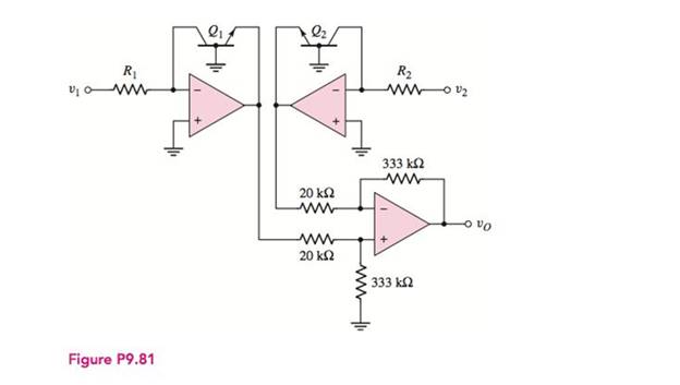
In the circuit in Figure P9.81, assume that
To show: The expression for the output voltageis
Explanation of Solution
Calculation:
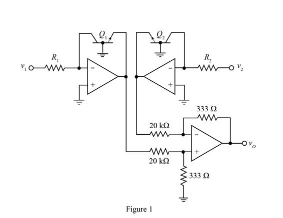
The given diagram is shown in Figure 1.
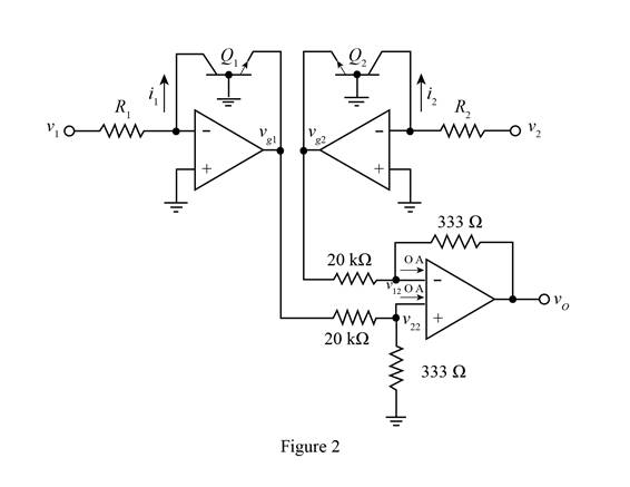
Mark the current directions, voltages and redraw the circuit.
The required diagram is shown in Figure 2
The expression for the voltage
For an ideal op-amp the voltage at both the input terminals are equal and is given by,
Substitute
Apply KCL at the inverting terminals of the lower op amp.
Substitute
The expression for the current
The expression for the current through the resistance
Substitute
The expression for the current
The expression for the current
Substitute
The expression for the transistor current is given by,
Substitute
Substitute
Substitute
Substitute
Therefore, theexpression for the output voltage is
Want to see more full solutions like this?
Chapter 9 Solutions
Microelectronics: Circuit Analysis and Design
Additional Engineering Textbook Solutions
Programmable Logic Controllers
Electrical Engineering: Principles & Applications (7th Edition)
Basic Engineering Circuit Analysis
Electric machinery fundamentals
Electric Circuits (10th Edition)
ELECTRICITY FOR TRADES (LOOSELEAF)


- Why do think the output voltage ?? resembles the input sinusoid?arrow_forwardQ9. Draw Zener regulator circuit to obtain regulated DC voltage 6.8 V. Considering input DC voltage in the range from 10V to 30V. Consider load resistance of 10KΩarrow_forwardWith capacitors in this Inverting Op-Amp, how should I find worst case values of Rin and Rf?arrow_forward
- Draw a three-phase full-wave fully controlled AC / DC converter circuit, describe the operating principle and write the integral correlation that gives the average value of the DC output voltage at any t1 momentarrow_forwardDesign the Clipper-Clamper circuit to perform the output waveform shown in figure below.arrow_forward2. What are all the effects of harmonics in power system? Define Total Harmonic Distortion (THD) and write its formula.arrow_forward
- sketch the output waveform and show the complete analysiisarrow_forwardassume ideal op-amp Find the center frequency, BW, & the gainarrow_forwardDefine the measured period in which the voltage drops to 63% of the peak-to-peak outputvoltage. What is the relationship of the measured period with the cut-off frequencies?Explain your answerarrow_forward
 Introductory Circuit Analysis (13th Edition)Electrical EngineeringISBN:9780133923605Author:Robert L. BoylestadPublisher:PEARSON
 Delmar's Standard Textbook Of ElectricityElectrical EngineeringISBN:9781337900348Author:Stephen L. HermanPublisher:Cengage Learning
 Programmable Logic ControllersElectrical EngineeringISBN:9780073373843Author:Frank D. PetruzellaPublisher:McGraw-Hill Education
 Fundamentals of Electric CircuitsElectrical EngineeringISBN:9780078028229Author:Charles K Alexander, Matthew SadikuPublisher:McGraw-Hill Education
 Electric Circuits. (11th Edition)Electrical EngineeringISBN:9780134746968Author:James W. Nilsson, Susan RiedelPublisher:PEARSON
 Engineering ElectromagneticsElectrical EngineeringISBN:9780078028151Author:Hayt, William H. (william Hart), Jr, BUCK, John A.Publisher:Mcgraw-hill Education,