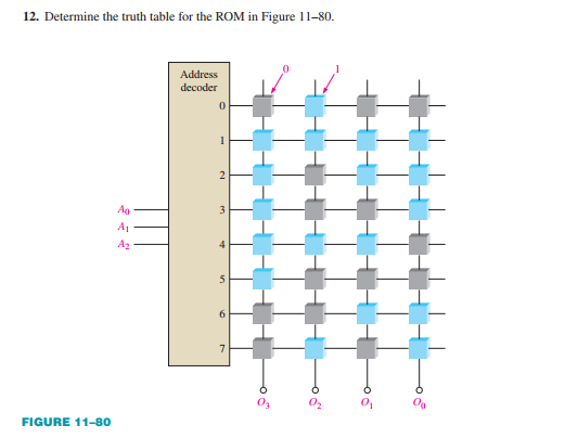
12. Determine the truth table for the ROM in Figure 11-80. Address decoder 2 Ag 3 A1 A2 7 FIGURE 11-8o


Q: A 74LS139 2-to-4 code is used to partition the memory space of an MC68008 into 4 quadrant, ROM, RAM,…
A: 74LS139 2-to-4 code: 74LS139 compares two separate 2-to-4 decoders in a single package. Features: It…
Q: Show the addresses and the contents of the ROM memory ( in HEX) after executing the following…
A: Answer: Given ROM memory stating address is 70H and DB directive will be stored in the ROM
Q: Which is a volatile memory : a) ROM b) BIOS c) PROM
A: Required: Which is a volatile memory : a) ROM b) BIOS c) PROM d) RAM
Q: Discuss the reading and writing of data to and from RAM.
A: RAM(Random Access Memory) is a primary, versatile memory. This memory device temporarily stores the…
Q: design a rom by using a address decoder, input buffer and or gate that stored value of 11 when…
A: Answer: I have given answered in the handwritten format
Q: Q10//Expand 64k x4 ROM to form 64k x 8 ROM.
A: Ans:) Give, We have 64K * 4ROM and we need to create 64K* 8 ROM.
Q: 3. If a ROM chip in some 8-bit microcomputer system starts with an address of 97C0H: while its end…
A:
Q: Short questions: Q. What is The Compressed form of Electrically Erasable Programmable Read-Only…
A: The Answer
Q: Define ROM and describe its purpose and identifying its most common application.
A: Actually, ROM is a one type o memory. It is used to stored the data.
Q: Design a 16-bit ALU from scratch following ISA format with a control unit in Logisim with…
A: Answer: I have given answered in the handwritten format
Q: The amount of ROM needed to implement at 4 bit multiplier is
A: The answer can be found by using the architecture of the Random Access Memory (RAM) as described in…
Q: 1. Clear the memory location ALPHA using data transfer instructions.
A: According to our guidelines we solve first one: Answer 1:…
Q: a rom by using a address decoder, input buffer and or gate that stored value of 11 when output line…
A: It is defined as a combinational logic circuit, whose purpose is to examine the address and raise an…
Q: 1. Write a VHDL description for 32x8 RAM. This RAM has the ports: clk, en,rdwr,address,…
A: 1.Answer: This question based on description of RAM when it manufactured process happen . So I have…
Q: Memories are normally classified according to their a. speed b. cost c. indexes d. both a and b
A: Given options - a. speed b. cost c. indexes d. both a and b
Q: How many data lines at required for a 8K x 8 ROM chip?
A: Given: ROM chip 8K × 8 To find: Number of data lines
Q: What is the size of my ROM if I want a maximum output of 6 bits? if possible draw a diagram
A: The correct answer for the question is given in the following steps for your reference.
Q: Design a memory module with 64 kilobyte ROM using 8K x 8 EPROM devices and similar sized writeable…
A: Introduction: EEPROM stands for electrically erasable programmable read-only memory and is a type of…
Q: Describe merits and demerits of linear decoding and fully decoding techniques used for designing…
A: Advantages: A linear model of communication is one way process in which one party is the sender…
Q: Draw a block diagram for 128x8 RAM *
A: Draw a block diagram for 128x8 RAM
Q: !!Please provide an explanation!! Fill in the blanks: A 64x8 ROM has __ input bits and __ output…
A: here in the question asks for a 64x8 ROM has how many input and output bits??
Q: Expansion of DRAM in memories is _____________.
A: The answer
Q: Q2/What is the range address for each memory chip in figure below? Draw the memory map. A14 A A13…
A: Answer: I have given answered in the handwritten format in brief explanation
Q: c) Find the ROM memory addresses of each of the following 8051 chips. i)AT89C51(or 8751) with 4KB…
A: Find the ROM memory address of each of the following 8051 chips. i) AT89C51(or 8751) with 4KB (ii)…
Q: Identify two basic characteristics Ram and ROM.
A: The storage space of a computer is called memory. The processed data and instruction for processing…
Q: In RAM and ROM, both are not having 1 byte of data bus Select one: O True False
A: Solution : - True
Q: Illustrate how three 2-Kbyte external ROM could be interfaced to the 8051 microcontroller
A: Illustrate how three 2-Kbyte external ROM could be interfaced to the 8051 microcontroller.
Q: State the differences between write bus cycle in memory in and read in Input/Output.
A: State the differences between write bus cycle in memory in and read in Input/Output.
Q: In a semiconductor ROM memory organized using 2-Dimensional addressing, the number of NMOS NOR gates…
A: Option c is correct Correct answer : c. 2^( The number of row address bits).
Q: 4. A RAM chip has a capacity of 64 bits. Draw the block diagram of the RAM clearly showing the total…
A: We need to answer -
Q: choose the correct answer In which of these ROM, data is permanently stored in it during the…
A: PROM is permanently stored in it during the manufacturing process . Advantages of memory ROM: The…
Q: Interface 4MB RAM memory with 80386SX microprocessor. Use 256Kx8 RAM ICs and 74LS138 decoder. The…
A: Given: We are given a problem in which 4MB RAM memory is interfaced with 80386sx microprocessor…
Q: uggest reasons why RAMs traditionally have been organized as only 1 bit per chip whereas ROMs are…
A: RAM (Random Memory Access) is one of the most fundamental units of the computer system. RAM is…
Q: Q1. Sketch a schematic for 8-word 2-bit masked programmed ROM where it stores the following…
A: Read-Only Memory is the…
Q: 3. Show the inputs and outputs for a 128 MByte memory with 32-bit read/write operations and byte…
A: The diagram is drawn in the next step :
Q: Draw a diagram of a static ROM in the form of 4 bit NMOS NOR array for two wor n10 and 1001.
A:
Q: RAM chip has a capacity of 64 bits. Draw the block diagram of the RAM clearly showing the total…
A: RAM of capacity :- 64 bits It contains 64*513 So it contain 32768 bytes. Total address line in RAM…
Q: Question Design a 1022*6 ROM memory by using a 256*4 Rom memory
A: Solution Design a 1022*6 ROM memory by using a 256*4 Rom memory we have 256*4 Rom memory where…
Q: Draw and explain the block diagram of the memory unit which is accessed by its content. Also explain…
A: Please find the answer below:
Q: Suggest reasons why RAMS traditionally have been organized as only 1 bit per chip whereas ROMs are…
A: RAM is also known as random access memory.
Q: - how a 32Kbyte ROM module can be c PROM chips, occupying the address ran ne following address…
A: Number оf аddress lines: 32K = 2* 2'° = 2'; 15 аddress lines (Ао - А14) Lines А15 — А19 аre used tо…
Q: Defines the address at which the programme will be placed in the microcontroller's memory.
A: INTRODUCTION: Memory is a resource-constrained key component in microcontroller-based bare-metal…
Q: Name three different applications where ROMs are often used.
A: Applications where ROM is used Read Only Memory (ROM) is non volatile memory. It is used for…
Q: If RAMXCS* is the chip select of a classified RAM module and ROMCS* is the chip select of the ROM…
A: BERR is the chip select signal. It is the control logic of digital circuits. Writing to ROM module…
Q: What does a dual-channel memory design serve?
A: THe answer is given below...
Q: Assembly What does "align 8,5" mean? Draw the data memory layout of the data memory starts at…
A: The ALIGN directive aligns the current location to a specified boundary by padding with zeros or NOP…
Q: Find address and data pins for the following memory organizations: 2048x2RAM
A: number of addressable locations = 2^n. number of addressable locations = 2048=2^n means =log(2048)…


Trending now
This is a popular solution!

Step by step
Solved in 2 steps with 1 images

- The 8051 memory map is subdivided into separate program/code and data memory.Describe a limitation with this approach and explain how the addition of an AND gatecan be used to resolve this problem. Briefly explain how this impacts on the memorymap.list the step needed to transfer a block of 15 words, starting address is 200 , by the DMA controller from the main memory .The answer must be 100% correct26. Memories are normally classified according to their a. speed b. cost c. indexes d. both a and b
- Design a memory module with 64 kilobyte ROM using 8K x 8 EPROM devices and similar sized writeable memory using 32K x 8 SRAM devices. The memory module must be compatible to the 8086 CPU module. Download the datasheets and show your design: Memory Map, Address allocation and decoding, and Timing specifications.What exactly is the working principle of direct memory access (DMA)?What does a dual-channel memory design serve?
- Find the capacity, address, and data pins for the following memory organizations. (a) 16K x 8 ROM (b) 64K x 4 DRAM!!Please provide an explanation!!Fill in the blanks: A 64x8 ROM has __ input bits and __ output bits.design a rom by using a address decoder, input buffer and or gate that stored value of 11 when output line is 0 do it right. i need the design