A) By Cascading a first-order op RC low-pass circuit with a first-order RC high-pass circuit, one can design a wideband bandpass filter. Design the filter for 3-dB bandwidth that extends from 200 Hz to 8 kHz. Select appropriate component values such that resistor values are between 10 k and 100 k. 1) Design 1: Add a voltage buffer (op amp with a gain of 1 V/V) between the LP and the HP circuits to prevent loading effect. 2) Design 2: Now add gain to the op amp (10 V/V) so that the filter midband gain is 20 B
A) By Cascading a first-order op RC low-pass circuit with a first-order RC high-pass circuit, one can design a wideband bandpass filter. Design the filter for 3-dB bandwidth that extends from 200 Hz to 8 kHz. Select appropriate component values such that resistor values are between 10 k and 100 k. 1) Design 1: Add a voltage buffer (op amp with a gain of 1 V/V) between the LP and the HP circuits to prevent loading effect. 2) Design 2: Now add gain to the op amp (10 V/V) so that the filter midband gain is 20 B

Introductory Circuit Analysis (13th Edition)
13th Edition
ISBN:9780133923605
Author:Robert L. Boylestad
Publisher:Robert L. Boylestad
Chapter1: Introduction
Section: Chapter Questions
Problem 1P: Visit your local library (at school or home) and describe the extent to which it provides literature...

Related questions

Question
if anyone can help me with this plz
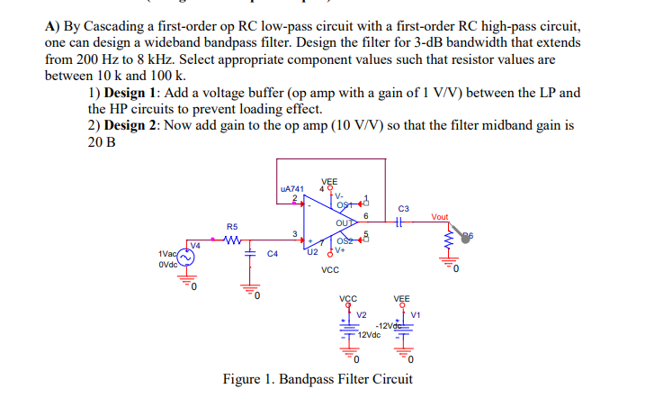
Transcribed Image Text:A) By Cascading a first-order op RC low-pass circuit with a first-order RC high-pass circuit,
one can design a wideband bandpass filter. Design the filter for 3-dB bandwidth that extends
from 200 Hz to 8 kHz. Select appropriate component values such that resistor values are
between 10 k and 100 k.
1) Design 1: Add a voltage buffer (op amp with a gain of 1 V/V) between the LP and
the HP circuits to prevent loading effect.
2) Design 2: Now add gain to the op amp (10 V/V) so that the filter midband gain is
20 B
VEE
40
V-
UA741
C3
6.
OUD
Vout
R5
3
OS
V4
02 V+
1Vac
Ovdc
C4
VCc
VEE
V2
V1
-12Vdc
12Vdc
Figure 1. Bandpass Filter Circuit
Transcribed Image Text:B) Simulate the above circuits using Orcad capture pspice.
1- Run Orcad capture CIS, open a new project from the file menu, and choose Analog
or Mixed Signal circuit Wizard
2- Draw the circuit of Design land save it (remember to add a ground)
3- In Pspice, select a new simulation profile: AC Sweep/Noise, Logarithmic, Start
freq= 1, End frequency= 100k, points per decade= 100
4- Name the output node Vout and add a voltage marker to the output
5- Run the simulation to verify the bandpass filter output (this is Gain (V/V) vs freq. in
Hz)
6- In Probe, from the menu. Trace -→Add Trace, the in the space of trace expression,
type DB(V(Vout)). This is the plot of 20log(Vout/Vi) vs frequency. Adjust the DB
axis to be between -30 dB and 5 dB (by going to Plot--- axis settings-Yaxis-user
defined)
7- Using the cursor tools (toggle cursor icon), verify the midband gain, lower and upper
3dB frequencies (fi and fr), center frequency fe, and roll-off in dB/decade. This is
Plot #1.
8- Repeat for steps 2 to 7 for Design 2 (Adjust DB zxis settings between -20 dB and 30
dB). This will give you Plot #2.
Expert Solution
This question has been solved!
Explore an expertly crafted, step-by-step solution for a thorough understanding of key concepts.

This is a popular solution!

Trending now
This is a popular solution!

Step by step
Solved in 3 steps with 3 images

Knowledge Booster


Learn more about
Need a deep-dive on the concept behind this application? Look no further. Learn more about this topic, electrical-engineering and related others by exploring similar questions and additional content below.Recommended textbooks for you
Introductory Circuit Analysis (13th Edition)
Electrical Engineering
ISBN:
9780133923605
Author:
Robert L. Boylestad
Publisher:
PEARSON

Delmar's Standard Textbook Of Electricity
Electrical Engineering
ISBN:
9781337900348
Author:
Stephen L. Herman
Publisher:
Cengage Learning

Programmable Logic Controllers
Electrical Engineering
ISBN:
9780073373843
Author:
Frank D. Petruzella
Publisher:
McGraw-Hill Education
Introductory Circuit Analysis (13th Edition)
Electrical Engineering
ISBN:
9780133923605
Author:
Robert L. Boylestad
Publisher:
PEARSON
Delmar's Standard Textbook Of Electricity
Electrical Engineering
ISBN:
9781337900348
Author:
Stephen L. Herman
Publisher:
Cengage Learning
Programmable Logic Controllers
Electrical Engineering
ISBN:
9780073373843
Author:
Frank D. Petruzella
Publisher:
McGraw-Hill Education

Fundamentals of Electric Circuits
Electrical Engineering
ISBN:
9780078028229
Author:
Charles K Alexander, Matthew Sadiku
Publisher:
McGraw-Hill Education

Electric Circuits. (11th Edition)
Electrical Engineering
ISBN:
9780134746968
Author:
James W. Nilsson, Susan Riedel
Publisher:
PEARSON

Engineering Electromagnetics
Electrical Engineering
ISBN:
9780078028151
Author:
Hayt, William H. (william Hart), Jr, BUCK, John A.
Publisher:
Mcgraw-hill Education,