(AB)' B. AB
Q: Simplify the following function and implement it using (i) NOR gates only (ii) NAND gates only (iii)…
A:
Q: Explain the circuit operation of positive and biased clipper circuit with neat sketch.
A:
Q: Q. Description a) Interpret the following circuit and Reconstruct using NAND gates CLO 1 1 F
A: a) It is given a logical circuit, we need to construct this circuit by using NAND gates. b) It is…
Q: 4. Draw a circuit using a NAND gate of the following function: A) F = (x'yz' + x'z) (xz' + xyz) (x +…
A: Given two Boolean functions.we need to implement them using nand gates.
Q: I Explain how to construct a NAND gate using Diode & Transistor.
A:
Q: Q8. In single pulse width modulation of single phase inverter, if supply voltage is 200 V DC and…
A: Given Supply voltage Vs=200V DC Given pulse width 2d =60° Then value of third harmonic ?
Q: Simplify the following functions, and implement them with two-level NAND gate circuits: (b)…
A: Given F(A,B,C,D) = A’B’C’D + CD + AC’D
Q: Represent the binary equivalent of 22 and 32 using by a creating 64-QAM constellation and pointing…
A:
Q: In your own words, explain why the circuit in Figure 3.2 is regarded as a logical inverter. Comment…
A:
Q: A network engineer in his office situated in Beijing China was trying to connect a server in…
A: Since he is unable to connect from Beijing to Singapore as well as to a server in his another office…
Q: Simplify the following functions, and implement them with two level NAND gate circuits: (A, B, C,…
A: It is given that: F(A, B, C, D)=AC′D′+A′C+ABC+AB′C+A′C′D′
Q: Implement the following expression as stated using only NAND gates. Y = AB + C'D + D'
A:
Q: Title If the emitter current of a transistor is 8 mA and B is 1100 of C , determine the levels of C…
A: Based on the given question we have value of emitter current Calculate Base and collector current
Q: Which one of the following is a microcontroller from Motorola? a) MC68HC05
A: The microprocessor which is designed by Motorola needs to be identified.
Q: A three phase bridge inverter is connected to star load of 10 2 resistance and operated from 200V DC…
A: Since you have posted a question with multiple sub-parts, we will solve the first three sub-parts…
Q: Re-design the circuit of one of the LED segments of the 7-segment display that you designed…
A:
Q: he gate of a MOSFET is insulated from the channel with a layer of SiO2. - True - False
A:
Q: (b) In your own words, explain why the circuit shown in Figure 3.2 is regarded as a logical…
A: The transistors consume power in idle condition because of the leakage current. Whereas , in case of…
Q: The small circle in the NAND gate represents
A:
Q: 2. (1) Prove that NOR gate is equivalent to a negative AND gate by constructing a simple circuit…
A: In a combinational circuit, the output only depends on the value of input as regards the previous…
Q: If you want to scale a 250µm gatewidth MESFET unit cell which is capable of producing 20dBm RF…
A: According to the question, If you want to scale a 250µm gate width MESFET unit cell which is capable…
Q: 6) Simplify the following functions, and implement them with two-level NAND gate circuits: (a) F(A,…
A: The given Boolean expression can be implemented with the help of NAND gate by simplifying the…
Q: Simplify the following functions and implement them with two-level NAND gate circuits: a. F(A,B,C,D)…
A: Given that Simplify the following functions and implement them with two-level NAND gate circuits:…
Q: AB+CD Use NAND gate (A+B)(C+D) Use NOR Gates (A+B').C.(B+C+D) Nor implementation
A: We are authorized to answer three subparts at a time, since you have not mentioned which part you…
Q: Implement circuit for following scenario using NAND gate only, draw circuit using multiplexer…
A: Let input 1 represents a low level of the chemical in any of the tanks, and 0 represents a normal…
Q: A single-phase, half-bridge inverter is supplied by upper half D.C source of 20 V and lower half D.C…
A:
Q: Q3: Compare between MOSFET and MESFET transistor in term of (Built on material, Oxide layer…
A:
Q: Q1.Simplify the following functions, and implement them with two-level NAND gate circuits: (a)…
A: The given function is: F = AC'D' + A'C + ABC + AB'C + A'C'D' The K- map can be drawn as: CD…
Q: a) Draw the energy band diagram of a MOSFET transistor, when -5 volts are applied to the drain…
A: a) We need to draw an energy band diagram of a MOSFET transistor when -5 V are applied to the drain…
Q: When the gate voltage VG is set to the same voltage as the source, what will be the maximum current…
A: In this question, When the gate voltage VG is set to the same voltage as the source, What will be…
Q: A CMOS NAND GATE has an input voltage 5v.The input current 2.5mA for high output and 3.6mA for low…
A: CMOS NAND gate is a type of logic gate in which two NMOS are connected in series and two PMOS are…
Q: 8. The collector leakage current in a transistor is 300 µA in CE arrangement. If now the transistor…
A: The solution is attached below.
Q: 8. A network interface port has collision detection and carrier sensing enabled on a shared twisted…
A: The given network interface has carrier sensing enabled on the given network and collision detection…
Q: design a 3-phase 50Hz inverter
A: Types of converters Rectifiers ( AC to DC Converter ) Chopper ( DC to DC Converter) Inverter ( DC…
Q: Design BCD to Excess 3 circuit using NAND gate
A: Let's take variables for BCD as A,B,C,D anf for excess-3 as W,X,Y,Z. Truth table: Decimal Input…
Q: Simplify the following functions, and implement them with two level NAND gate circuits: F (A, B, C,…
A: It is given that: F (A, B, C, D)=A′B′C′D+CD+AC′D
Q: Question 4 Draw the following function using only NAND gate F(A,B,C) = A+(C+B') %3D
A:
Q: Q What is the difference between NAND gate and negative AND gate'
A: A Not gate is a logic gate whose output is invert of input applied. OR gate is a logic gate whose…
Q: Please simplify the functions of each and implement two-level nand and nor circuit. Thank you! F=…
A: we need to simplify the functions of each and implement two-level nand and nor circuit. and F=…
Q: Design a BCD to gray code converter and implement using PLA
A:
Q: Simplify the following functions, and implement them with two-level NAND gate circuits: F(A, B, C,…
A: The symbol of the two-input NAND gate is as follows, if A and B are the inputs the out = (AB)'
Q: Specify the MCBS required for three (3) ACs, three (3) WHs and 20 (twenty) Socket outlets ?
A: For an AC the the output power will be 2300W that means 10 to 15 current is needed, so for three ACs…
Q: I want presentation about mosfet / Jft
A: It is needed to explain the basics about about MOSFET.
Q: (b) In your own words, explain why the circuit shown in Figure 3.2 is regarded as a logical…
A:
Q: Please explain it to me and simplify this function and draw the circuit using two-level Nand and Nor…
A:
Q: ۱۰ تعليقات ل لفئة Re-design the circuit of one of the LED segments of the 7-segment display that you…
A:
Q: Show Two level implementation of the following expression using only or and not Gates AB+CD Use…
A: Boolean operations involve the implementation of basic logic gates. The logic gate operations…
Q: 2. Design an excess-3-to-BCD code converter with efficient implementation.
A: 2. The excess 3 to BCD code converter is found below: The logic diagram:
Q: Resistor Transistor Logic (RTL) circuits Explain( AND,NAND,NOR,OR AND NOT )
A:
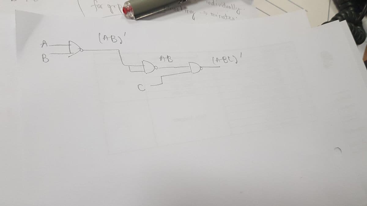
Show how this NAND will be implemented on IC.
Step by step
Solved in 2 steps with 2 images
- In the given circuit R1 = 15kohm R2 = 3kohm Vs-24V Is = 2mA What kohm should the RL value be for maximum power transfer?VEE =-12V, VCC = 12V, R1=9800 ohm, R2 = 3300 ohm, RC = 1800 ohm, RE = 970 ohm, B = 100 Calculate IB , VC , VB , VCE , VEDirections on file below. You can use determinant, reduce row echalant form whatever you see fit