(b) For a MOSFET amplifier circuit shown in Figure Q.1, the transistor parameters are: Vr = Vas(TH) = 1.5V, k = 0.5 mA/V², ra = co, all junction and stray capacitances are neglected except Cwo. The circuit is to be designed such that: • The Vaso = 2.79 V • The input impedance, Z,= 155 k2 • The small signal voltage gain, A, = • The lower -3dB frequency associated with C1, fici = 20 • The upper -3dB frequency associated with Cwo, fito - 10 By performing DC and ac analysis, (i) Draw the ac equivalent circuit at mid-band frequency. (ii) Determine the value of the resistors Rị and R2. IVERITI TEKMOaGI MALAYSIA (iii) Determine the value of the transconductance, gm. (iv) Determine the value of the resistor Rp. VERSITIT (v) Calculate Vpso. (vi) Determine the value of C1 and Cwo. ALA
(b) For a MOSFET amplifier circuit shown in Figure Q.1, the transistor parameters are: Vr = Vas(TH) = 1.5V, k = 0.5 mA/V², ra = co, all junction and stray capacitances are neglected except Cwo. The circuit is to be designed such that: • The Vaso = 2.79 V • The input impedance, Z,= 155 k2 • The small signal voltage gain, A, = • The lower -3dB frequency associated with C1, fici = 20 • The upper -3dB frequency associated with Cwo, fito - 10 By performing DC and ac analysis, (i) Draw the ac equivalent circuit at mid-band frequency. (ii) Determine the value of the resistors Rị and R2. IVERITI TEKMOaGI MALAYSIA (iii) Determine the value of the transconductance, gm. (iv) Determine the value of the resistor Rp. VERSITIT (v) Calculate Vpso. (vi) Determine the value of C1 and Cwo. ALA

Chapter25: Television, Telephone, And Low-voltage Signal Systems
Section25.1: Television Circuit
Problem 5R: From a cost standpoint, which system is more economical to install: a master amplifier distribution...

Related questions
Question
Transcribed Image Text:at mid-band frequency.
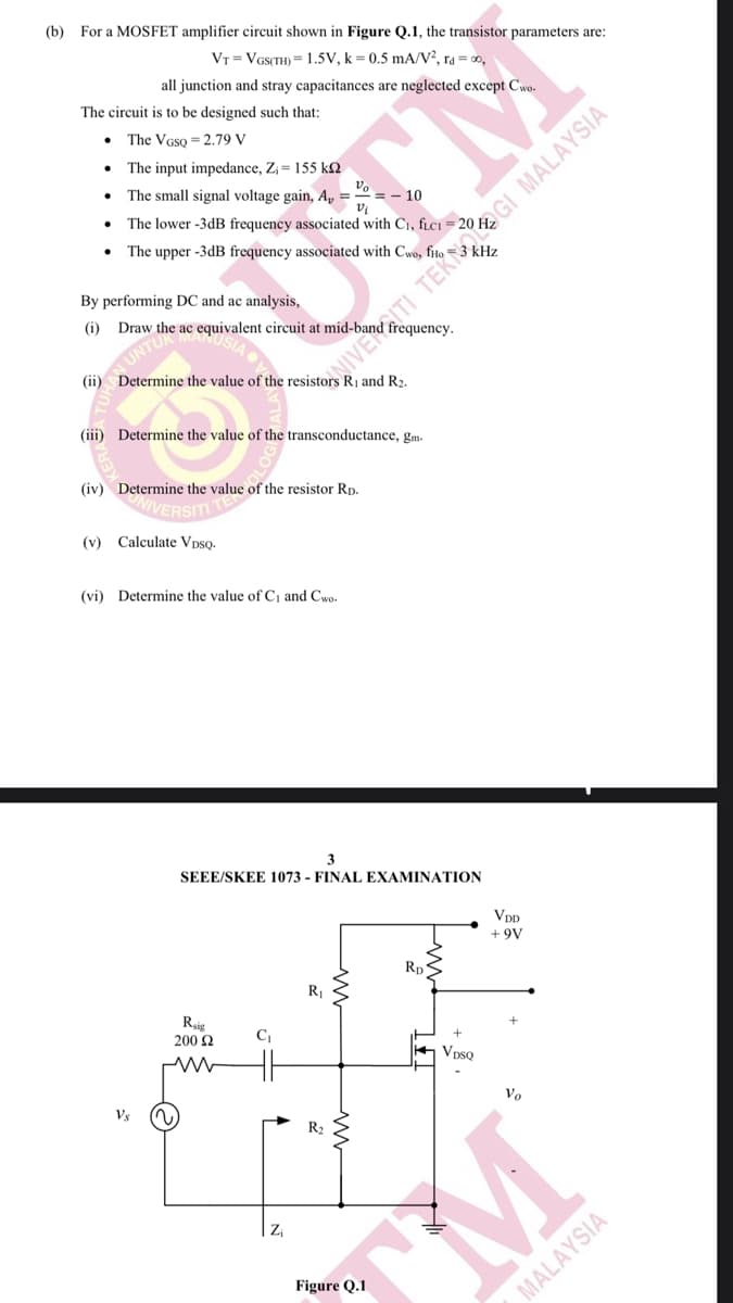
(b) For a MOSFET amplifier circuit shown in Figure Q.1, the transistor parameters are:
VT = VGS(TH) = 1.5V, k = 0.5 mA/V, ra= 0,
all junction and stray capacitances are neglected except C.
The circuit is to be designed such that:
The VGso = 2.79 V
The input impedance, Z= 155 k
The small signal voltage gain, A, =
:- 10
The lower -3dB frequency associated with C1, fLCI = 20 1
la
The upper -3dB frequency associated with Cwo, fto
By performing DC and ac analysis,
(i) Draw
v the ac equivalent circuit at
UNTU
(ii) Determine the value of the resistors R1 and R2.
(iii) Determine the value of the transconductance, gm-
(iv) Determine the value of the resistor Rp.
IVERSITI TE
(v)
Calculate VpsQ.
(vi) Determine the value of C, and Cwo.
3
SEEE/SKEE 1073 - FINAL EXAMINATION
Vpp
+ 9V
Rp
R
Rig
200 2
K VpsQ
Vs
Vo
R2
Zi
Figure Q.1
M
MALAYSIA
TI TEKNOOGI MALAYSIA
Expert Solution
This question has been solved!
Explore an expertly crafted, step-by-step solution for a thorough understanding of key concepts.

Step by step
Solved in 4 steps with 4 images

Knowledge Booster


Learn more about
Need a deep-dive on the concept behind this application? Look no further. Learn more about this topic, electrical-engineering and related others by exploring similar questions and additional content below.Recommended textbooks for you
EBK ELECTRICAL WIRING RESIDENTIAL
Electrical Engineering
ISBN:
9781337516549
Author:
Simmons
Publisher:
CENGAGE LEARNING - CONSIGNMENT
EBK ELECTRICAL WIRING RESIDENTIAL
Electrical Engineering
ISBN:
9781337516549
Author:
Simmons
Publisher:
CENGAGE LEARNING - CONSIGNMENT