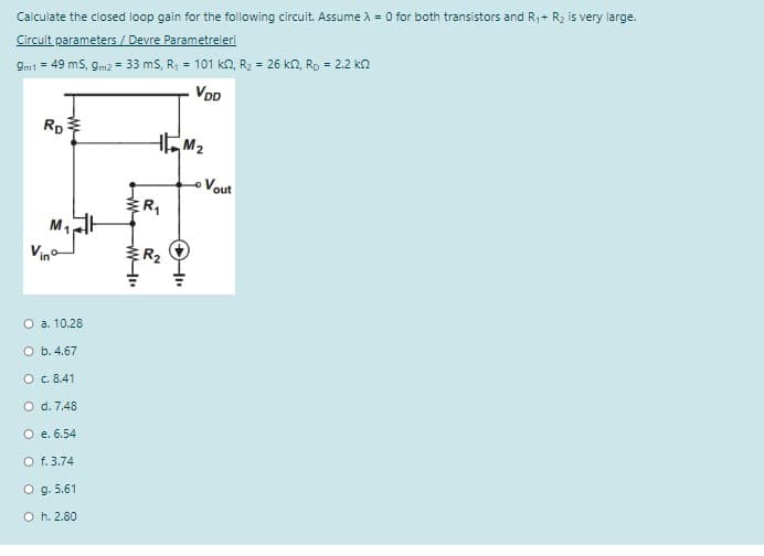
Calculate the closed loop gain for the following circuit. Assume A = 0 for both transistors and R,+ R2 is very large. Circuit parameters / Devre Parametreleri 9m1 = 49 ms, 9m2 = 33 ms, R, = 101 kn, R2 = 26 k, Ro = 2.2 kn VDD %3D Rp Vout Vino R2


Q: 3E Problem 1. (P1) Three op-amps are connected in cascade configuration. An 80 microVolts signal is…
A: For the above given question we need to derive the value of input voltage for 2nd opamp and the…
Q: Figure snows a differential amplifier connection constant current to provide a large value of…
A:
Q: Consider the circuit shown in the Figure. Let Vcc = 4.4V and VBg = 2 The transistor parameters are:…
A: The solution is given below
Q: The op-amp datasheet for amplifier shown in Figure 3 has Zin-2.3 MN, Zout = 90 Q and Aol = 150,000.…
A:
Q: RI Vo RL VI Figure 1 In the Figurel, let RI = 4kN, Rf =12k2, and V1 = 2V. The load resistance RL of…
A:
Q: +15 V 25 mV, LF157A Vout pp 3 kN -15 V 150 2
A:
Q: Design a self-bias that operates for maximum output signal swing. The amplifier will have a voltage…
A: Here we need to find the dc parameter of the bjt by analyzing the given parameter. Small-signal…
Q: Qr: Choose the correct answer. Each question weighted (2 marks). The circuit of Figure below uses…
A:
Q: An operational amplifier with voltage-series feedback configuration shown in Figure Q3(c) has the…
A: We need to find out Gain with feedback and unknown resistance.
Q: 4. For the collector-feedback configuration, determine: a. IB b. IC +16 V с. VС 3.6 k2 270 k2 Vc Ic…
A:
Q: 02 (B):- For the non-inverting operational amplifier circuit shown in Figure (3). 1) Derive the…
A:
Q: 3. a) Describe the classification of system based on stability. b) Convert the following figure to a…
A: a) In simple words, a system is said to be stable if its output is under control. If a system…
Q: Vin Iout Rs = lookn RL = 5 K2 AI Ri= 45kn Ra =5 ke For the amplifiers open-loop gain, Az= lo00 AlA…
A: Given data RS=100kΩRL=5kΩR1=45kΩR2=5kΩAI=1000 AARin=1kΩRout=25kΩ a) From the figure it is clear…
Q: Q6/ For the voltage feedback network of Figure below, determine: (a) Ic 9 30 V (b) Vc 8.2 k2 (c) VE…
A:
Q: V. IN VOUT R1 ww R1 R2 Ay = 1+ R2 Use R2=1000, R1=1kN, Vs=12V. The closed loop gain of the…
A: Given, a non-inverting amplifier Closed-loop gain = Av=1+R1R2 R1 = 1000 ohms & R2 = 100 ohm The…
Q: Design a DC-DC boost converter to meet the following: the input voltage is 10 V, the required output…
A: Chopper is a dc to dc converter. There are mainly three types of chopper Buck converter Boost…
Q: Please choose the best answers for the folloiwng statement: Isolation amplifiers are a form of…
A: In this question we will write about isolation amplifier....
Q: CE amp with dual Supply O +5 V Re C3 10 ΚΩ 330 2 220 ΚΩ R1 Rg Rout R3 100 kN RE 16 k2 -5 V Problem:…
A: Let us first do the dc analysis of the circuit. In this case, all the capacitors are open-circuited.…
Q: (c) For the Schmitt trigger circuit shown below, calculate the values of the upper threshold point…
A:
Q: Q5) Calculate the gain without and with feedback for the FET amplifier circuit with the following…
A: Given data:R1 = 100 KΩR2 = 25KΩRL = 15KΩRD = 12KΩgm = 4000ms
Q: +16 V 3.6 kN 270 k2 Vc B = 120 1.2 k2 (b) 1. For the collector-feedback configuration of figure 2…
A: By referring to figure we can find IB as IB=Vcc-VBERB+βRC+REIB=16-0.7270 kΩ+120(3.6kΩ+1.2kΩ)=18.09…
Q: Q5) Calculate the gain without and with feedback for the FET amplifier circuit with the following…
A:
Q: Design an Instrumentation Amplifier with Common Mode Rejection Ratio 80 dB minimum, differential…
A: According to the question, we need to design an Instrumentation Amplifier with Common Mode Rejection…
Q: 3B Problem 1. (P1) Three op-amps are connected in cascade configuration. An 80 microVolts signal is…
A:
Q: Calculate the gain without and with feedback for the FET amplifier circuit with the following…
A: Calculate the gain without and with feedback for the FET amplifier circuit with the following…
Q: Note: answer (4) four questions only Q5 Calculate the gain without and with feedback for the FET…
A: given R1= 100KΩR2 = 25 KΩRL = 15 KΩRD= 12kΩ gm = 4000 ms
Q: Estimate the magnitude of the loop gain of the circuit shown below. The op-amp has the following…
A: Given:rd=1 MΩro=100 Ω Aol=105R1=39.70 kΩand R2=1.88 kΩ
Q: b) An ideal transconductance amplifier is connected as shown in Figure Q3.b. The overall voltage…
A: Ideal transconductance amplifier has infinite output impedance and infinite input impedance as shown…
Q: An inverting operational amplifier circuit is manufactured from an op-amp, two resistors of values 4…
A: It is given that: R1=4kohmR2=10kohmVin=3V
Q: A- The point where amplifier high frequency gain has dropped 30% is a. the crossover point. b. the…
A: The point where amplifier high frequency gain has dropped 30% is called cross over point.
Q: Draw the circuit diagram for a voltage amplifier model with the following parameters: Source…
A: We need to draw the circuit diagram for a voltage amplifier model with the following parameters.…
Q: Calculate the gain without and with feedback for the FET amplifier circuit with the following…
A: Given data:R1=100 kΩR2=25 kΩ RL=15 kΩRD=12 kΩgm=4000 ms
Q: +9 V - = 20 k2 P,-B,-75 47 k2 Rc 47 k2 Vo Q1 Q2 V,= 2 mV 43 k2 9 V
A:
Q: Q3: Prove that: 1:- Ac-Current gain of collector feedback amplifier is a proximally Rp/Rc.…
A: For the given question We have to prove : Ac-current gain of collector feedback amplifier :…
Q: For circuit in Figure 4, if the maximum frequency is 1 Mrad/sec and the op-amp slew rate is SR=0.25…
A: Given data, Frequency f=1 Mrad/sec =12π×106 Hz Slew rate SR =0.25V/μs…
Q: Calculate the closed loop gain for the following circuit. Assume A = 0 for both transistors and R,+…
A: The small signal equivalent of the given circuit is
Q: Question 1 a. Compute Vo/Vs parametrically. Explain briefly the operation principle of the circuit.…
A: NOTE: As there are multiple questions, as per the guidlines solving first three questions The…
Q: Q2 R R-A VIN) O A2 VOUT VIN(+) O R R+ 4 Figure Q2 (a) (a) Figure Q2 (a) shows the circuit diagram of…
A:
Q: For the follower circuit in the figure below, consider k = 0.3x10⁻³ , rd = 100kOhm, VT = VGS(TH) =…
A:
Q: Calculate the common-mode output voltage and A, voltage gain for the circuit below, where V = 5mV,…
A:
Q: Q2. Given the circuit configuration below, Vcc=VEE=6V, R = 2kn Rc = 6kn, Re = 5kn, Rb = 0, Rw = 2002…
A: The circuit is given as Diffential voltage gainAd=α2R+RC2re+RW2
Q: An operational amplifier with voltage-series feedback configuration shown in Figure Q3(c) has the…
A:
Q: 3E Problem 1. (P1) Three op-amps are connected in cascade configuration. An 80 microVolts signal is…
A: For the above given question we need to derive the value of input voltage of the second stage of the…
Q: A transistor used in a common collector circuit as shown in figure has following set of…
A:
Q: Determine the maximum theoretical efficiency of RC-coupled class-A amplifier as shown in Figure…
A: It is asked to determine the maximum theoretical efficiency of an RC-coupled class-A amplifier.
Q: For the series-fed class A power amplifier shown in Figure Q3, assume that Vcc= 18 V, B = 26 and RB…
A:
Q: QUESTION 1: The differential amplifier in Figure P11.4 is biased with a three-transistor current…
A: The circuit diagram is shown below, The transistor parameters are,β=160VBE(on) = 0.68 VVA = ∞
Q: Assuming and ideal current source with infinite output impedance for the current source l, draw…
A: consider the given question;
Q: 3. An OpAmp-based amplifier is shown below: R1=R2=15kN RL R2 R2 R R (1) Assume that the OpAmp was…
A: "According to the Company's policy, we solve only the first part of the question, since each part is…
Q: +15 V 25 mV LF157A Vout pp 3 k2 -15 V 150 2
A: The detailed solution is provided below.


Trending now
This is a popular solution!

Step by step
Solved in 2 steps with 2 images


- In the circuit given in the figure, Vcc = 15V, R1 = R2 = 10k ohm, RE = 1k ohm, RL = 0.5k ohm and transistor parameters are given as VBE = 0.7V, beta (dc) = beta (0) = 100. According to this;a) Calculate the values of DC bias currents and voltages (I (BQ), I (CQ), V (CEQ)).b) Using the hybrid model of the transistor, draw the small signal equivalent circuit of the circuit.c) Derive the input impedance expression of the circuit and calculate its value.d) Derive the voltage gain expressions A (vi) and A (VG) and calculate its value.e) Derive the current gain expression A (i) = I (0) / I (i) and calculate its value. I sent you question's image. Thank you..1) Calculate the DC parameters listed in Table 1 for Q1 and Q2 for the MOSFET amplifier circuit shown in the figure. 2) Calculate the AC parameters. Compute the gain by completing the small signal analysis. Draw the input and output signals to scale.Vs=100 mV peak-to-peak, 1 kHz sine signal, Kn=0.4mA/v^2 ,Vt=1V , λ=0.01V^-1 Make the DC analysis of the above given mosfet amplifier circuit. Simulation to tableWrite down the measured values and mathematical calculation results. (The valueswith the units.)DC Parameters ,Measured value ,Calculated ValueVGETCVGSVDVDSIDb. Draw the small signal model for the AC analysis of the circuit. Find the gm, ro, Av values.c. Show the Vs input signal and the Vo output signal of the circuit on the oscilloscope. Volt/div of channels andSpecify time/div values.
- The multistage amplifier circuit of Figure Q.2(b) have the following parameters:Q1 and Q2 : β = 200, VBE = 0.7 V, VT = 26 mV , VA = ∞Given that ICQ1 = 2 mA and VCEQ1 = 2 V. (i) Determine the value for RB4. List the assumption/approximation made in the analysis.(ii) Sketch and label the small-signal hybrid-π equivalent circuit at midbandfrequency range.(iii) Calculate the small signal hybrid-π model parameters: gm and rπ for Q1 and Q2. Then, determine Zi2 and Zo.For the BJT amplifier circuit of figure below with the following parameters:β = hfe ≈ 250, re= 20.3Ω, and ro = 1/hoe ≈ ∞ Ω, Zb= 50.26KΩ determine:(a) Draw the Ac equivalent circuit in re- model and hybrid model.(b) hie, , Zi , and Zo'(c) Av using h- model.(d) Avs and ac output voltageFor the 2 circuits shown above, βnpn = 100, βpnp = 50, VDO = 0.7 V, R2 = 150 kΩ, and RB = 12 kΩ Using the ac small-scale signal analysis, determine for each circuit: a) The voltage gain (Av = vout/vin) b) The input resistance (Rin) c) The output resistance (Rout)
- Draw the equivalent circuit for a common-emitter bipolar transistor amplifier andderive suitable formulae for the amplifier current gain, voltage gain and power gain.Neglect bias,decoupling and coupling componentsInstruction/s: Draw, Illustrate and label your schematic diagram before solving the problem.2.) Given a Collector -Feedback Biased transistor circuit with voltage at common collector is +10v ,base resistor is 100k ohms, Collector resistor is 10k ohms and Base current is 8.38 micro ampere, ,Voltage at Base-emitter junction is 0.7v. Determine Beta DC , Collector current and Voltage at collector-emitter junction. These might help as a guide to answer the problem...A base voltage of four volts is applied to an NPN bipolar junction transistor. A twenty kilo ohm resistor is linked to the base, while a hundred kilo ohm resistor is connected to the collector. The Collector is powered by a six volt supply voltage. Assume the transistor is in active mode, with a fifty common Emitter current gain(β).(i) Utilize the dc equivalent model of the transistor to draw the circuit design.(ii) Calculate the Collector current (IC) and the Base current (IB) .ii) Locate/determine the result (VCE).
- a.) Consider a two-BJT configuration in Figure 1. You may assume that both transistors are the same with the same β, VBE,on = 0.7 V, and VCE,EOS = 0.3 V. Determine the minimum voltage VBE that will turn ON both Q1 and Q2. b.) Using the BJT small-signal model given in Figure 2, determine the AC current gain Ai = iout/iin for the circuit given in Figure 3. Assume ro >> rπ. You may assume that β is large.In the circuit given in the figure, Vcc = 15 V, R1 = R2 = 10kΩ, RE = 1KΩ, RL = 0.5kΩ and transistor parameters are given as VBE = 0.7V, ßdc = ß0 = 100. a. Calculate the values of DC bias currents and voltages (IBQ, ICQ and VCEQ). b. Draw the small signal equivalent circuit of the circuit using the hybrid model of the transistor. c. Derive the input impedance expression of the circuit and calculate its value. d. Derive the AVI and AVG voltage gain expressions and calculate their values. e. Derive the current gain expression AI = I0 / Ii and calculate its value. Compare this value you have calculated with the value you will calculate using the expression Aİ = Zi AVI / RL.2. A load of 8Ω is supplied by a single-switch Direct Current (DC) chopper with an inputvoltage of 40V. The switching frequency is 800Hz, the duty ratio is 0.4, and thetransmission voltage drop of the transistor is 2.4V a. Draw the chopper circuit presented in the question b. Find the switching period with the duty time of BJT c. Draw the load voltage, load current, BJT current, BJT voltage along two periods d. Find the output voltage. Is the achieved load voltage the average value or the effectivevalue e. Find the output power f. Find the average value and effective value of BJT current g. Find the power loss of BJT h. Find the DC source current i. Find the circuit efficiency