Calculate the gate to source voltage VGs for a NMOS transistor with B 2200 HA/V, V=1 V and operating in saturation with a transconductance gm 5 mS. %3D %3D Draw the small signal equivalent circuit model valid in the mid-band frequency range for the circuit shown in Figure 1 and identify the kind of amplifier formed by the NMOS transistor M1. Clearly state any assumption. Using two transistors nominally identical to MI and the configuration shown in Figure 1, design a common source voltage amplifier with improved gain. Draw the mid-band frequenci
Calculate the gate to source voltage VGs for a NMOS transistor with B 2200 HA/V, V=1 V and operating in saturation with a transconductance gm 5 mS. %3D %3D Draw the small signal equivalent circuit model valid in the mid-band frequency range for the circuit shown in Figure 1 and identify the kind of amplifier formed by the NMOS transistor M1. Clearly state any assumption. Using two transistors nominally identical to MI and the configuration shown in Figure 1, design a common source voltage amplifier with improved gain. Draw the mid-band frequenci

Introductory Circuit Analysis (13th Edition)
13th Edition
ISBN:9780133923605
Author:Robert L. Boylestad
Publisher:Robert L. Boylestad
Chapter1: Introduction
Section: Chapter Questions
Problem 1P: Visit your local library (at school or home) and describe the extent to which it provides literature...

Related questions
Question
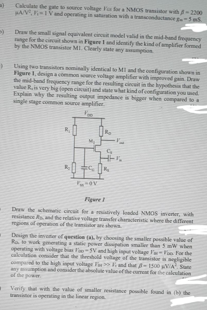
Transcribed Image Text:Calculate the gate to source voltage VGs for a NMOS transistor with B=2200
HA/V, V= LV and operating in saturation with a transconductance g 5 mS.
Draw the small signal equivalent circuit model valid in the mid-band frequeney
range for the circuit shown in Figure 1 and identify the kind of amplifier formed
by the NMOS transistor Ml. Clearly state any assumption.
Using two transistors nominally identical to MI and the configuration shown in
Figure 1, design a còmmon source voltage amplifier with improved gain. Draw
the mid-band frequency range for the resulting circuit in the hypothesis that the
value R, is very big (open circuit) and state what kind of configuration you used.
Explain why the resulting output impedance is bigger when compared to a
single stage common source amplifier.
R,
Rp
M1
out
Cs
R,
Rs
I'ss =0V
Figure I
Draw the schematie cireuit for a resistively loaded NMOS inverter, with
resistance Rp, and the relative voltage transfer characteristic where the different
regiens of operation of the transistor are shown.
Design the inverter of question (a), by ehoosing the smaller possible value of
Rp, to work generating a static power dissipation smaller than 5 mW when
operating with voltage bias l'oD -5V and high input voltage FH= VDD. For the
caleulation consider that the threshold voltage of the transistor is negligible
compared to the high input voltage ViH >> Vi and that B= 1500 µV/A. State
any assumption and consider the absolute value of the current for the calculation
of the power.
Verify that with the value ef smaller resistance possible found in (b) the
transistor is operating in the linear region.
Expert Solution
This question has been solved!
Explore an expertly crafted, step-by-step solution for a thorough understanding of key concepts.

Step by step
Solved in 4 steps

Knowledge Booster


Learn more about
Need a deep-dive on the concept behind this application? Look no further. Learn more about this topic, electrical-engineering and related others by exploring similar questions and additional content below.Recommended textbooks for you
Introductory Circuit Analysis (13th Edition)
Electrical Engineering
ISBN:
9780133923605
Author:
Robert L. Boylestad
Publisher:
PEARSON

Delmar's Standard Textbook Of Electricity
Electrical Engineering
ISBN:
9781337900348
Author:
Stephen L. Herman
Publisher:
Cengage Learning

Programmable Logic Controllers
Electrical Engineering
ISBN:
9780073373843
Author:
Frank D. Petruzella
Publisher:
McGraw-Hill Education
Introductory Circuit Analysis (13th Edition)
Electrical Engineering
ISBN:
9780133923605
Author:
Robert L. Boylestad
Publisher:
PEARSON
Delmar's Standard Textbook Of Electricity
Electrical Engineering
ISBN:
9781337900348
Author:
Stephen L. Herman
Publisher:
Cengage Learning
Programmable Logic Controllers
Electrical Engineering
ISBN:
9780073373843
Author:
Frank D. Petruzella
Publisher:
McGraw-Hill Education

Fundamentals of Electric Circuits
Electrical Engineering
ISBN:
9780078028229
Author:
Charles K Alexander, Matthew Sadiku
Publisher:
McGraw-Hill Education

Electric Circuits. (11th Edition)
Electrical Engineering
ISBN:
9780134746968
Author:
James W. Nilsson, Susan Riedel
Publisher:
PEARSON

Engineering Electromagnetics
Electrical Engineering
ISBN:
9780078028151
Author:
Hayt, William H. (william Hart), Jr, BUCK, John A.
Publisher:
Mcgraw-hill Education,