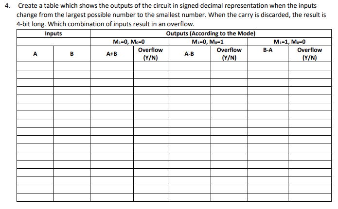
Create a table which shows the outputs of the circuit in signed decimal representation when the inputs change from the largest possible number to the smallest number. When the carry is discarded, the result 4-bit long. Which combination of inputs result in an overflow.


Q: Plot the following discrete-time signals over the range -10 <ns 10: i. 6[n-3] ii. u[n-3] iii. r[n-3]…
A: Requirements:- Since you needed only third part. of this question Solution :- Please see the code…
Q: Design a sequential circuit that outputs 2’s complement of a bit sequence. The bit sequence will be…
A:
Q: Question Construct a 3*8 Decoder using only 5*32 Decoder(s)
A: Note: There are multiple questions are given in one question. According to the rule, you will get…
Q: 1. Design an N-bit ALU with 4-bit ALUControl signal that fulfills the following operations.…
A: To design an N-bit ALU with 4-bit ALU Control Signal for the following: ALUControl…
Q: 3- Design a 2-to-1 multiplexer by using UDP. The select signal is s, inputs are i0, il, and the…
A: The select signal is s, inputs are i0,i1, and the output is out. If the select signal s=x, the…
Q: Q11/Chose the correct answer for the output Q3 of the following circuit ( Assume that A= 1010101010,…
A: Here depending upon the value of output of D and T flip flop, the input to JK flip flop will be…
Q: Design 4 bit left/right rotation circuit that specifies the number of bits in the rotation by a…
A: Lets see the solution in the next steps
Q: 4. A 4-to-1 multiplexer is defined by the following symbol and truth table. f $i So So Wo Wo 1 W1 f…
A: Find Your Answer below
Q: Design a sequential circuit that outputs 2's complement of a bit sequence. The bit sequence will be…
A: Sequential Circuit: The sequential circuit is a special type of circuit that has a series of inputs…
Q: Plot the result of the convolution between the two signals shown below.
A: Step by step solution is given below-
Q: An analog signal is changed to a binary coded form by what circuit?
A: Analog to Digital Converter (ADC) is a circuit that is used to convert the analog signals such as…
Q: In CRC if the data unit is 100111001 and the divisor is 1011 then what is dividend at the receiver?…
A: The question is on in CRC if the data unit is 100111001 and the divisor is 1011, what will be the…
Q: Design a combinational circuit that uses 4-bit adders and 2-to-1 MUXes. Given two 8-input signed…
A: Hey there, I am writing the required solution of the questin mentioned above. Please do find the…
Q: For a resolution of 0.032 V and an analog sample voltage of 4.030 V, complete the table below:…
A: Below I have provided the handwritten solution of the given question
Q: The circuit shown in figure performs addition as well as subtraction. If 4-bit binary numbers…
A: If s=1 it act as an subtractor
Q: 02: Assemble the binary bits of the "PCM" signal below into a DPSK waveform, in the case of the…
A: I will explain it in details,
Q: logic diagram for the comparison of two 4-bit binary and Q,Q, Q, Qo ?
A: Comparison of two 4 bit binary numbers Here I considered my P3,P2,P1,P0,as A3,A2,A1,A0 and…
Q: The Companding occurs only when; a. Small signals are attenuated and Large signals amplified b.…
A: Companding --> Companding is the process of compressing the audio signal prior to transmission…
Q: Given the analog signal shown in figure, what are the 8-bit pulse code modulated values that will be…
A: Pulse Code Modulation (PCM): PCM is one of the encoding techniques used for converting analog data…
Q: Course: Digital Electronics How to implement a full subtractor using a decoder IC 74138? and why…
A: IC 74138 is the 3*8 demux, which can be used in the full subtractor. Full subtractor has the three…
Q: In a 7-segment decoder, displaying a digit 4 makes the Blank 1 segment(s) off. Write segment/s in…
A: The segment of seven segment display is following way
Q: Design a sequence detector of the pattern 0100 where the circuit accepts a serial bit stream *X" as…
A:
Q: Assume that a digital circuit represents numbers in 8-bit. In this circuit what is the 1’s and 2’s…
A: Answer to the following question
Q: Build a system that converts a 3 bit number to its 1’s complement form using encoder and decoder…
A: converts a 3 bit number to its 1's complement form using encoder and decoder
Q: The power spectral density shows how the power is distributed over the frequencies included in a…
A: The power spectral density shows how the signal level is distributed across the frequency domain.
Q: Draw the logic diagram for the comparison of two 4-bit binary numbers P3 P2 P, Po and Q, Q, Q, Q, ?
A: The solution for the above-given question is given below:
Q: Build a system that converts a 3 bit number to its 1’s complement form using encoder and decoder…
A: According to your specifications, I created the system for you. Consider an 8x3 encoder and feed it…
Q: type ard using an illustration. 100 ADD R1, R2 101 OR R3,R2.R1 102 Jump 107 103 SW R 104 Jump 106…
A: It is defined as a low-level language because it directly works with the internal structure of CPU.…
Q: umber to its 1's complement
A: For according your requirement i done that system for you Consider 8x3 encoder and give input to…
Q: Answers are at the end of the chapter. 1. Determine the sum (E) and the output carry (Cout) of a…
A: I have answered both the questions and have uploaded image for the step wise solution. In the first…
Q: The Line Coding scheme that shows the best behavior (among the following) with a long sequence of…
A: While doing programming in any programming language, you need to use various variables to store…
Q: Q1: Answer the following as true or false 7- De-multiplexer is used to connect a single source to…
A: Statements regarding digital logic device are given here, and we have asked which of them are…
Q: Show using diagram the contents of the six output frames for a synchronous TDM multiplexer that…
A: Given:
Q: If a decoder decodes a 4-bit pattern what is the maximum number of output wires it can have and how…
A: Please give positive ratings for my efforts. Thanks. ANSWER As decoder has the input and output…
Q: The Nyquist theorem for noiseless channel states that the capacity in bits per second of a channel…
A: This question comes from Computer Network which is a paper of computer science. Let's discuss it in…
Q: Design a signed n-bit multiplier.
A: Design a signed n-bit multiplier.
Q: output
A: Answer: Since the Data Encryption Protocol (DES) has been shown to be vulnerable to extremely strong…
Q: Find the bit rate of an analog signal modulated at a speed of 9000 bauds and carrying 3 bits per 2…
A:
Q: Implement a digital module that send the same output values as defined in the following truth table…
A:
Q: Q6/Chose the correct answer for the output Q3 of the following circuit ( Assume that A= 1010101010,…
A: Answer: The correct answer for the output Q3 of the following circuit where A = 1010101010 B=…
Q: Choose the most simple SOP expression from the K-map shown. AB 00 01 11 10 00 1 01 CD 11 10 Select…
A: EXPLANATION: The k-map minimizes the boolean expression on the basis of the groups that are formed…
Q: What is the minimum and maximum number of outputs in a 4-input binary decoder
A: For n bits (or n inputs) we can have total 2n combinations (i.e. 2n outputs) e.g. for n = 2,…
Q: What is the size of my multiplier if I want a maximum output of 6-bits? create a diagram
A: A binary multiplier (multiplier) is a combinational logical circuit used to perform mutiplication on…
Q: The given function table is for an eight-bit ALU circuit with Bounded Signed Integers in Two’s…
A: Here below i a modifying into for 4 bit:…
Q: Complete a truth table that has 3 inputs (A, B, and C) and one output (F). F=1 whenever the binary…
A: Complete a truth table that has 3 inputs (A, B, and C) and one output (F). a. F=1 whenever the…
Q: An analog signal is digitized and stored in a file. For digitizing with 3 bits, if data rate is 56,4…
A: An analog is digitized and stored in a file. for digitizing with 3 bits, if data rate is 56,4 Kbps…
Q: Since Fclk=64 Khz in the diagram given below, what is the frequency at the Y output when A=0, B=1?
A: let us see the answer: Since Fclk=64 Khz in the diagram given below, what is the frequency at the Y…
Q: LA signal x(n) is graphically shown below. Show the graphical representation of the signals -3x(n')…
A: From the given graph, we can observe that, x(n) = 4+nfor n < 04for 0≤n≤40for 4 < n
Digital Logic Design
4-bit Binary Adder / Subtractor
please answer the whole sheet

Step by step
Solved in 2 steps with 2 images


- Data represented in ________ is transmitted accurately between computer equipment from different manufacturers if each computer’s CPU represents real numbers by using an IEEE standard notation.Create a table which shows the outputs of the circuit in signed decimal representation when the inputs change from the largest possible number to the smallest number. When the carry is discarded, the result is 4-bit long. Which combination of inputs result in an overflow.Consider this 1-bit ALU design, as shown in class (note that the rounded rectangles controlled by Ainvert, Binvert, and Operation represent multiplexers): If I want Result to be the result of a - b, then what value do each of these other inputs need to be? Ainvert : 0 or 1 Binvert : 1 or 0 CarryIn: 1 or 0 Operation : 00 , 01, 10, 11 which one ?
- Write a program that acquires data from a data source and calculates and displays the Discrete FourierTransform associated with that data. In this case, the Arduino will generate a signal, that is sampled by the ADC and then sent to the computerover the serial port. The Arduino code is : int lookup_index = 0; #define SIN_FREQ 100 long sin_freq = SIN_FREQ; #define LOOKUP_ARRAY_SIZE 128UL #define PWM_RESOLUTION 8 #if PWM_RESOLUTION <= 8 #define PWM_t uint8_t #else #define PWM_t uint16_t #endif PWM_t *lookup_array; // lookup array for sin(2pi f t) PWM_t lookup_array1[LOOKUP_ARRAY_SIZE] = { 127, 133, 139, 146, 152, 158, 164, 170, 176, 181, 187, 192, 198, 203, 208, 212, 217, 221, 225, 229, 233, 236, 239, 242, 244, 247, 249, 250, 252, 253, 253, 254, 254, 254, 253, 253, 252, 250, 249, 247, 244, 242, 239, 236, 233, 229, 225, 221, 217, 212, 208, 203, 198, 192, 187, 181, 176, 170, 164, 158, 152, 146, 139, 133, 127, 121, 115, 108, 102, 96, 90, 84, 78, 73, 67, 62,…Design a circuit that has two inputs X, and S, where X represents an 8-bit BCD number, S is a sign bit. The circuit has one output Y, which is the Binary representation of the signed-magnitude BCD number. A negative output is represented in the Binary 2’s- complement form. You need to think of two design alternatives. Submission guidelines: 1. You should write a report that at least contains the following sections: 1. Problem definition. 2. Design alternatives : 2.1. Alternative 1 block diagram 2.2. Alternative 2 block diagram 3. Design selection criteria 4. Detailed circuit design of the selected alternative. 5. Verilog modules, and simulation results for all modules, and for the whole circuit of the selected alternative .Design a sequence detector of the pattern 0100 where the circuit accepts a serial bit stream *X" as input and produces a serial bit stream *2° as outputWhenever the bit pattern *0100* appears in the input stream, it outputs 2 = 1: at all other times, 2 = Q Overlapping occurrences of the pattern are also detected,
- What is the size of my multiplier if I want a maximum output of 6-bits?Given five inputs (a, b, c, d, e) connected to 8051’s port P1 and P2 with : P1.0 = a, P2.0 = b, P1.3 = c, P2.7 = d et P1.6 = e. Outputs S0 and S1 are connected to P3.0 and P3.1 respectively as shown in the figure below. We propose to realize the following logic S0 = a.b + c.d + e.(a.b + a.b) S1 = c.b + d + e.a.bDesign a circuit that takes three bits, X2, X1, X0 as input and produces one output, F. F is 1 if and only if 2<=X<=5 when X = (X2, X1, X0) is read as an unsigned integer. For example, if X2=1, X1=0, and X0=0, then the unsigned binary value is 100, which is 4, so the output would be 1. Your Assignment For This Problem Includes the Following Design the necessary circuit using Logisim to implement the situation described above. Use Kmaps for simplification. Be VERY careful to get the correct functions for your output before simplifying and designing the circuit with Logisim. You should minimize the circuit. Your circuit should have three inputs and one LED output. All inputs (X2, X1, X0) and output (F) should be labeled (in Logisim, not by hand). Please use these names to indicate the inputs and output so all projects are consistent. You should also include your name as a label on the circuit. Test your circuit to be sure it is working correctly.
- The Line Coding scheme that shows the best behavior (among the following) with a long sequence of ones (i.e. the bit 1) in terms of synchronization and baseline wandering is _____: Select one: a. Both NRZ-I and Unipolar NRZ b. Any of the mentioned choices are correct c. Both NRZ-L and NRZ-I d. Unipolar NRZ e. Bothe NRZ-L and Unipolar NRZ f. Polar NRZ-I g. Polar NRZ-L h. None of the mentioned choices is correctSuppose that four different four-bit numbers are to be taken from memory and added by the circuit discussed in class. How many CLEAR pulses will be needed? How many TRANSFER pulses? How many LOAD pulses?The fundamental distinctions between synchronous and isochronous connections will be explicated, and an instance of each will be presented.