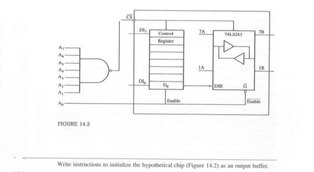
CS DI, 7A 78 Control 74LS245 Register A7 A6 As A4 IA IB Dlo Do DIR A Enable Enable Ao FIGURE 14.2 Write instructions to initialize the hypothetical chip (Figure 14.2) as an output buffer.


Q: c) ( >) If a CPU has 24 address lines and 24 bit data bus. Show the design of L3 (direct mapped…
A: please check the solution below
Q: A computer employs RAM chips of 512 x 16 and ROM chips of 1024 x 8. The computer system needs 4K…
A: The answer is
Q: Q8/Assume that the microprocessor can directly address 64K with a R/W' and 8 data pins The memory…
A: option b
Q: er a 48-bit word long instructions. It has 200 registers, each of which is 48 bits long. It needs to…
A: Here in this question we have given a 48 bit architecture machine with 1 word long…
Q: 154. Device controller is the controller of the computer system that contains a. buffers b.…
A: Each I/O device controller has a local buffer and set of special registers. The device controller is…
Q: RS AND EMBED CONTROLLERS AND EMBEDDED SYSTEMS-1 General > If a file register, x, is set to Ox01,…
A: Let's first understand what is the use of Comf function and why we need it . Now as the name…
Q: 3. If a ROM chip in some 8-bit microcomputer system starts wita an address of 97C0H while its end…
A: If a ROM chip in some 8-bit microcomputer system starts with an address of 9700Hwhil its end…
Q: Identify if possible the type of addressing modes for the following instructions. 1. MOV ES, DX
A: The addressing mode for MOV ES,DX is as follows.
Q: PSR Register C Register initial values R1 RO R2 R3 R4 R5 Ox DAE0C1 Instruction MOV R11,R1,ROR #2.…
A: Instructions and their meaning: MOV R11, R1 moves content of R1 into R11. ROR #2 right rotates the…
Q: 1. Clear the memory location ALPHA using data transfer instructions.
A: According to our guidelines we solve first one: Answer 1:…
Q: Assembly to Binary 2 An LC-3 assembly language program contains the instruction LEA R6, Z The symbol…
A: Explaination, As we know that the value stored at Y ie at x3005 will be the 16 bit binary code for…
Q: Q. No. 6: If the memory or an I/0 interface could not able to respond in the duration of a read and…
A: ANSWER:-
Q: ubject: Computer Organization and Architecture (COA) Question: The state diagram with interrupt…
A: Solution Address content 0234056H 3000 023405bF 20000 Let salary be 3000 and t% tax…
Q: the microprocessor accepts the iterrupt by activating the e On receipt of the-signal, the…
A: 11. INTA 12. HLDA 13. Instruction cycle 14. DS
Q: Design a CPU System that combines and connect memory system, ALU, registers and control unit. The…
A: Design a CPU System that combines and connect memory system, ALU, registers and controlunit. The CPU…
Q: Design memory decoder for a system having a total of 2GB RAM divided in sub memory modules of 512MB.…
A: Design memory decoder for a system having a total of 2GB RAM divided in sub memory modules of 512MB.…
Q: 5) instruction performing a word-size add operation: (note: caution for the constant and address…
A: Lets see the solution.
Q: Q8/Assume that the microprocessor can directly address 64K with a R/W' and 8 data pins The memory…
A: Please check the solution below
Q: 1.The 8085 microprocessor is an 8-bit processor available as a 40-pin IC package and uses V for…
A: Please upvote me please. I need it badly please. 1. The 8085 microprocessor is an 8-bit processor…
Q: na MIPSZY processor, when is PCincremented by 4? O After the data memory is accessed. O Before the…
A: MIPS is a RISC computer, and that means all orders have the same length: 32 bits. So for every…
Q: c) () If a CPU has 24 address lines and 24 bit data bus. Show the design of L3 (direct mapped cache)…
A:
Q: Question please zoom in to see image What is the value of EAX and EDX registers after these…
A: Ans: The value of EAX and EDX registers after these instructions are executed is: mov eax, 6 cdq mov…
Q: 厂 Assembly LOADI RO, -1 LOADI R1. -3 ADD RO, RO Memory Loc Machine Code 00101111 00111101 01000010…
A: The Answer is
Q: Level 2 of cash memory usually built outside the CPU. single register is needed for the CPU to run…
A: While doing programming in any programming language, you need to use various variables to store…
Q: e AVR instruction set includes instructions for addition, subtraction, and multi e corresponding…
A: Hey there, I am writing the required solution of the questin mentioned above. Please do find the…
Q: Question 1: Logic Path and Delay A. Calculate the time to execute the following instructions. B.…
A: for addi addi accesses instruction memory once, register read or write twice , ALU once, adder once…
Q: d 2K bytes of ROM along with interface unit of 128 registers each. A memory mapped I/0 cont The two…
A: The Answer is
Q: The Control Bus make a signal to: communicate with the ALU generate timing the actual instruction…
A: The control bus make a signal to Bus requests Basically control bus permits the CPU to receive or…
Q: 102. Completion of operation to the CPU of the computer system is told by a. buffers b. interrupt c.…
A: Given that, Completion of operation to the CPU of the computer system is told by a. buffers b.…
Q: Select the correct option about below mentioned characteristics: 1. Decode the instructions to…
A: Actually, computer consist of 5 main essential parts ALU Memory unit Control unit Input Outpput…
Q: Figure Q3 shows the memory mapped I/O of a LPC1768 microcontroller. It shows that the…
A: Given The answer is given below.
Q: Design 8086's memory system consists of 512K bytes of RAM and 128K bytes of ROM using the devices…
A:
Q: This question assumes the machine architecture at the right. Note the stack pointer register, SP, is…
A: Sel0, And, MDRinWMFC, R1out, MARin, WRITE, Yin
Q: MULTIPLE CHOICE 7) According to computer architecture: a. Data is exchanged between components…
A: To Do: To choose the correct option.
Q: The 16F84A PIC core is the microprocessor inside the microcontroller centered around the ALU: False…
A: The core is the microprocessor present inside the micro controller centered around the Arithmetic…
Q: A computer employs RAM chips of 512 x 16 and ROM chips of 1024 x 8. The computer system needs 4K…
A: The number of chips needed in RAM is 2048 /256 = 8 chips. 2048 = 211 256 = 28 The number of chips…
Q: Identify if possible the type of addressing modes for the following instructions. 1. MOV EDX, [EAX…
A: The way of specifying data to be operated by an instruction is said to be addressing mode.…
Q: In technique, The /O module and main memory exchange data directly without processor involvement. a.…
A: Answer : Correct answer is option ( d ) direct Memory Access(DMA).
Q: Q47/ Design maximum RAM system using the following RAM chips ( the memory chip is enabled only when…
A: It is defined as a system call provides mapping in the virtual address space of the calling process…
Q: B- Design microprocessor 8086 memory system consisting of 1M byte, using • 128KX8 memory chips • 2:4…
A: Explanation :
Q: Design a CPU System that combines and connect memory system, ALU, registers and control unit. The…
A: the solutions is given below :
Q: Answer B part only! a) Draw a block diagram of a microprocessor based system interfaced with 8255,…
A: Question:
Q: A micro-instruction format has micro-ops field which is divided into three subfields F1, F2, F3 each…
A: The micro-instruction consists of three fields. Fields of microoperation F1,F2,F3 Status bits on a…
Q: To interface 1.5us access time memory chip with 5MHZ CLK 8086 processor, need to insert - wait…
A:
Q: Memory a) MOV DI, 561 MOV AX, 11H ADD AX, [DI] ADD AX, [DI+2] 22 11235H i. Determine the memory…
A: Below i have answered:
Q: Q8/Assume that the microprocessor can directly address 64K with a R/W' and 8 data pins The memory…
A: Given: Assume that themicroprocessor can directlyaddress 64K with a R/W' and 8 data pins The memory…
Q: Chap 14. Interfacing to external memory 1. Interface two 16 Kbytes RAM chips (16K x 8) with the…
A: It is defined as one of the basic type of microcontroller, designed by Intel in 1980’s. This…
Q: Module Organization Eхample: 512 words by 512 bits How a memory module Memory address register (MBR)…
A: Hey there, I am writing the required solution based on the above given question. Please do find the…
Q: An instruction is stored at location100 with its address field at location 110. The address field…
A: On the basis of instructions given to a computer, it performs various tasks. An instruction is made…

Step by step
Solved in 2 steps with 2 images


- If a microprocessor has a cycle time of 0.5 nanoseconds, what’s the processor clock rate? If the fetch cycle is 40% of the processor cycle time, what memory access speed is required to implement load operations with zero wait states and load operations with two wait states?AssemblyWhat does "align 8,5" mean? Draw the data memory layout of the data memory starts at 0x20000000Area myData, DataAlign 4a DCB 1b DCB 2c DCB 3Align 8,5d DCB 5Question)E Explain a XYZ method of transferring data from the computer's RAM to another part of the computer without processing it using the CPU. As a sound card may need to access data stored in the computer's RAM, but since it can process the data itself, XYZ is a means of having a peripheral device control a processor's memory bus directly. It permits the peripheral, such as a UART, to transfer data directly to or from memory without having each byte (or wordhandled by the processor. Draw a diagram of the unit used in XYZ and how data is transferredusing this method.
- Consider a CPU which operates with 20Mbyte/s operating speed. The CPU is operating on program control mode of I/O and it has to transfer data of 20 bytes from it. The data is transferred byte wise. Size of the Status register is 2 bytes. What is the total time needed to perform the data transfer?We want to build a word organized main memory of 8 GB for a 32-bit CPU architecture composed of word organized memory modules of 30-bit address and 8-bit data buses each. a) Draw the interface of the main memory by clearly indicating the widths of the buses. b) Howmanymemorymoduleswouldbenecessarytobuildthememorysystem? c) Design the main memory internal organization built out of the above memory modules (use multiplexers and/or decoders as needed) by clearly indicating the widths of the used busses d) CanweusethismemorysystemasRAMfortheCPUinProblem1?Explainyouranswer.Q2: Choose the correct answer 1. Suppose that a system uses 32-bit memory words and its memory is built from 16 1M × 16 RAM chips. How large, in words, is the memory on this system? A) 8M B) 16M C) 32M D) 64M 2. The __________ converts machine instructions of 0s and 1s into control signals. A) microprogram B) control store C) microsequencer D) control unit 3. Memory that is accessed by searching for content is called: A) read only memory. B) erasable memory. C) associative memory. D) virtual memory. 4. Binary code that has addresses relative to the location where the operating system has loaded the program in memory is called _______________ code. A) loadable B) absolute C) relocatable D) movable 5. Which phase of a compiler generates syntax errors? A) Lexical analysis B) Syntax analysis C) Parsing D) Semantic analysis 6. Cache memory is typically positioned between: A) the CPU and RAM. B) the CPU and the hard drive. C) ROM and RAM. D) None of these is correct. i need it ASAP please…
- Please explain how prioritizing the I/O queue above the process execution queue might improve performance. If the I/O is interrupted, who knows what will happen. To what extent this will reduce the maximum burst rate of the CPU is unclear. I don't think I understand what you're getting at.please explain these bullets more In memory-mapped I/O devices and main memory share the same address space. ⚬Each I/O device has its own reserved block of memory. ⚬Memory-mapped I/O therefore looks just like a memory access from the point of view of the CPU. ⚬Thus, the same instructions to move data to and from both I/O and memory, greatly simplifying system design. In small systems the low-level details of the data transfers are offloaded to the I/O controllers built into the I/O devices.Suppose a computer using fully associative cache has 224 bytes of byte-addressable main memory and a cache of 128 blocks, where each cache block contains 64 bytes.Q.) What is the format of a memory address as seen by the cache; that is, what are the sizes of the tag and offset fields?
- Suppose a computer using fully associative cache has 224 bytes of byte-addressable main memory and a cache of 128 blocks, where each block contains 64 bytes.Q.) What is the format of a memory address as seen by cache; that is, what are the sizes of the tag and offset fields?A multiprocessor consists of 100 processors, each capable of a peak execution rate of 2Gflops. What is the performance of the system as measured in Gflops when 2% of the code is sequential and 98% is parallelizable?Research how the MMU is used to translate a virtual address to a real physical address. Write a 200 word summary and discuss how the MMU supports this functionality, how an MMU is used in an operating system, and finally, write the pseudo code logic to support how the MMU translates and maps addresses.