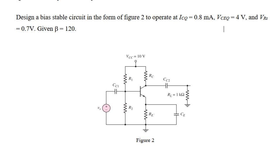
Design a bias stable circuit in the form of figure 2 to operate at Ico= 0.8 mA, VCEQ =4 V, and VRE = 0.7V. Given ß = 120. Vcc = 10 V RC R1 Cc2 RL = 1 k2 R2 CE RE Figure 2 wwH ww


Q: 20 KQ R1 10V Vin Vout -10V Figure 3: The above given circuit in Figure 3 is that of a noninverting…
A: We know hyteresis width for non inverting opamp .
Q: For the following self-bind cåveuit, find equivalent circuit acpas Bale aud ground. •Vcc RI Baul 3Re
A: The Thevenin equivalent across base and ground:
Q: on A semiconductor with more charge carriers is: Select one: O a. Less conductive O b. More…
A: 1. Answer: b. More conductive Because conductivity of a semiconductor is directly proportional to…
Q: V 40V R2 82k R1 2.7k Q1 Q2N2222 R5 R4 1.2k Figure 2: Voltage-divider DC bias configuration
A: Since, you have asked multiple questions here, we can answer only one of them at a time. Kindly,…
Q: Q2. A JFET has the following parameters: IDSS = 32 mA; VGS (off) = -8V; VGS = -4.5 V. Find the value…
A: The Given is JFET parameters IDSS=32mA; VGSoff=-8v; VGS=-4.5v To find the drain current.
Q: thermistor
A:
Q: What is the name of the circuit given below? PR1 v 5.9976V PR2 v 5.9976V R1 1kQ D1 V1 7.5V 3 1kHz 0°…
A:
Q: 12 I D1 R1 1k R2 1k D2
A: We need to analyse the given circuit
Q: аc sn Int motor runs om a 400 V supply w mature current of 25 eed at which it will r pply when…
A:
Q: 25 - Bağlantı sıcaklığını hangi formülle hesaplanır? By which formula is the junction temperature…
A: The junction temperature is calculated by the formula TJ = TA + (R θJA × PD )
Q: For the fixed -bias Configurahion of Figure 1, delermine : a) I BQ b) Ice c) VCEQ O1GV Ice Figure 1…
A: “Since you have posted a question with multiple sub-parts, we will solve first three sub-parts for…
Q: The diode (blue line) should be at -10V not -8V
A: The Diode-based circuit can be designed in LTspice by selecting the general diode and changing the…
Q: for the circuit shown in figure , a silicon is used B=40 find the value of Vo and the regiion of…
A:
Q: he total resistance of a rotary potentiometer = 120Ω Maximum angle = 230°degree, the supply voltage…
A: Equivalent resistance find out: To solve above problem, one should know how to find equivalent…
Q: Ideal voltage source should have • zero internal resistance O • infinite internal resistance O •…
A:
Q: +12v Current Limiting Resistor Switch M. Single or LED Array Ic C RB IB Motor Lamp Heater VN O…
A: A transistor is a type of a semiconductor device that can be used to both conduct and insulate…
Q: Given the zener voltage at 9V and the zener power at 1W, what is the range of allowable values of Iz…
A:
Q: Solve the emitter voltage (VE) of Figure 612. Vc 8. R1 3.3k2 Beta = 110 VEE R2 -12V 3.9kQ Figure 612…
A: In this circuit, find the value of emitter voltage VE We know Assume VBE = 0.7 V
Q: Consider the circuit shown. Is ER3 DE + V R1 R4 R = 3.4 kQ and R3 = 5.0 kN. E= 10V. The diode has…
A:
Q: Design a voltage-divider bias circuit in Figure 1 with a gain of 5. Assume the following values: R1=…
A:
Q: Q6/ Explain mode of the transistor circuit shown below. Re 5 ΚΩ 12 V ig B + + RB Va VBE E 8 V RE VE…
A:
Q: 31. If the voltage measuring function of a linear NTC thermistor is Vout = -1.4T( "C) + 4.35 V, the…
A:
Q: Q2. The stabilizer current of the thyristor in the circuit is below 100mA and the delay time of the…
A:
Q: * What is wrong with this circuit? R₁ 10 kn V₁ 24 V 1N4744A 1 15 V The zener is open. O The zener is…
A: We need to check whether diode is on or off
Q: saturation? What minimum value of VIN is necessary for saturation? Assume VCE(sat) = 0 \ FIGURE 4-59…
A:
Q: Determine the approximate value of drain current (Ip) of Figure 55. VDD 21V 910ka 2.2ka 10mA V =-…
A: The solution is given below The answer is option b
Q: for the circuit shown below: The lower reference threshold 10v vin=5 sinwt -10v 3 kOhm 1 k Ohm
A: A voltage reference is an electrical component or circuit that generates a constant DC…
Q: + 12v Current Limiting Resistor R Switch M Single or LED Array R Ic RB Ig I Motor Lamp Heater VN O B…
A: Hello. Since your question has multiple sub-parts, we will solve the first three sub-parts for you.…
Q: 2. a) Define the function of each opamp given below. b) Calculate V.. 18K ww 36K 6K 6K 2 V Div 12K…
A:
Q: The diagram shown below is: Vss (OV) $10 B p+ S " D p-type substrate D p+ p+ Vo (2.5 V)
A: It is a CMOS INVERTER CIRCUIT
Q: 30. The value of collector current Ic is (а) 5.14 mA (b) 4.94 mA ( c) 28.5 μΑ
A:
Q: Based on electric circuit shown in Figure 2. Determine whether the LED 1 and LED 2 is "ON" or "OFF"…
A: we know that for an opamp the voltages at both terminal of opam are equal. For V1= 2 volts. The…
Q: D1 Vo Si VS R1 VSINE V1 VS=112 Volts, R1=28,5k and V1=8Volts Find Vo (in volts) while Diode 1 is not…
A: Find the Vo when diode is not working ?
Q: What is wrong with this circuit? * R1 Σ10 ΚΩ 2 HIL V₁ 24 V 4.790 R₂2.5 kn RL 1 15 V O The zener is…
A:
Q: Instructions: Determine the indicated parameters from the given circuits and show the complete…
A:
Q: (b) 0 Identify and the model the mathematical function to plot the following diagram shown in Figure…
A: clc;close all;clear; t = 0:0.01:8;x = t.*(t>=0&t<1) + (-t+2).*(t>=1 & t<2) +…
Q: 3. Calculate the current through the Zener diode for the given values of load resistance in this…
A:
Q: 12V R1 2 Vout R2 VREF +88 8 5V Volts -12V Determine the output voltage, Vout when: R1=10000,…
A: We need to find out output voltage for given circuit
Q: Solve the emitter current (I;) of Figure 612. vc 8V R1 3.3ka Beta = 110 VEE R2 -12V 3.9kQ Figure 612…
A: Solve for the emmiter current
Q: Draw a circuit diagram with electrical symbols for the figure below. 100 N + 50 N 12 V 10 µF
A: When current will start flowing through 12 V battery, 50 Ω resister will be in series after that…
Q: A battery with EMF of 4V and an internal resistance, r = 0.80 is connected to a load resistance R =…
A:
Q: What is wrong with this circuit? * R12 10 ΚΩ + V₁ 24 V 2 1N4744A 1 15 V O The zener is open. O The…
A: Given Vs = 24V , Rs = 10k , RL = 2.5k
Q: Q3. Draw the output voltage waveform for each circuit including the voltage values. (Ideal model)…
A: "According to the company's policy, we will provide an answer for the first part of the question…
Q: 29. The vollage applied across an electric press was reduced by 50%. The power consumcd by thc prcss…
A: Given Voltage across electric press was reduced by 50% . Voltage, V2 = 0.5 V1 where V1 is voltage…
Q: Figure 4 b) Figure 5 shows the silicon base BJT with a Rc = 1 k, R3 = 10 kn, Vcc = 11 V, VBB = 6 V,…
A:
Q: (2) Labäi If a FET has a pinch off voltage = . -1V , ID=1mA, and Vgs=0V, What is ?the value of IDSS…
A: Given: Pinch off voltage, Vp=-1 V Gate source voltage, Vgs=0 V Drain current, ID=1 mA
Q: PRELIMARY 1. For the circuit in Figure 1, the transistor is biased so that Ico is 10 mA and Vez is 8…
A: Thevenin's Theorem According to Thevenin's Theorem, any linear circuit, no matter how complicated,…
Q: V1 R1 8Ω E Xc 16 N
A: Given I3 = 5A across 10 ohm resistor. So voltage across the resistor is V3 = 5×10 = 50V Voltage…
Q: 20-30 V 20 Ω 7,5 MO Vo
A:

Step by step
Solved in 2 steps with 2 images


- A 10 V Zener diode is used to regulate the voltage across a variable loadresistor. The input voltage Vs varies between 13 and16 V. The loadcurrent (??) varies between 10 and 85 mA. The minimum Zener current is15 mA. Findi. The maximum value of Rsii. The maximum power dissipated by the Zener diode, using the value ofRs.The mode of operation for the D-MOSFET is Select one: a. the ohmic region only b. the enhancement mode only c. both the depletion and enhancement modes d. the depletion mode onlyNOTE: FOR ALL CIRCUITS SHOWN IN THIS QUIZ ASSUME THAT: β= 100 (for all transistors) ; Early voltage equal to infinity. 1.- In the circuit of figure Nº A, the secondary voltage Vs is 15 volts rms with a frequency of 60 Hz, R equal to 100 Ohms and C equal to 1000 microfarads. The diodes are silicon (Vd = 0.7 volts) and the Zener diode is 15 volts. Determine:a) The magnitude of the ripple voltage at Cb) The Magnitude of the Peak Inverse Voltage (PIV) for D1 and D2
- Can someone explain this problem step by step? How do I know is in active more, or saturation mode? If you know those conditions , how do we suppose to work it out. Also why step 2 and 3 the current are almost the sameA loaded zener regulator has a VZ of 11 V with IZ equal to 23 mA, with IZK equal to 0.25 mA, ZZ equal to 8 Ω and a PD (max) equal to 1 W. The value of the resistance R is equal to 32 Ω. Determine the values of the output voltage with IZK and IZM. Get the value of the minimum load resistance that can be used to keep the zener diode regulating.Prepare the comparison table for the Power semiconductor devices 1)Integrated gate-commutated thyristor (IGCT) 2) Static induction thyristor (SITH) 3)Static induction transistor (SIT) .(Symbol, VI characteristics, Application, Voltage & Current rating)
- 2. Given:VCC: 16 voltsRB1: 7000 ohmsRB2: 50 ohmsRB3: 50 ohmsRB4: 1500 ohmsB=beta: 100RE: 750 ohmsRC: 500 ohmsVCE: ? voltsGiven the schematic below and the following assumptions: Forward Voltage of D1 and D2 are 5V VBE,ON = 0.7V and VCE,Sat = 0.6V Do the following: Equate R2 to 500Ω. Assume that the BJT is operating in Forward Active mode and that both diodes are on. Verify if the assumptions are correct. If not correct, determine what state the BJT (Forward Active, Saturation, Cutoff or Reverse Active) and diodes (On or Off) are in. Equate R2 to 1,000,000Ω. Assume that the BJT is operating in Forward Active mode and that both diodes are on. Verify if the assumptions are correct. If not correct, determine what state the BJT (Forward Active, Saturation, Cutoff or Reverse Active) and diodes (On or Off) are in.Silicon BJT (β=120) and Germanium BJT (β=120) VCE in circuitCalculate its value. Comment the circuit
- topic: diodes the data in the table is obtained using electronics workbench simulation. answer the following blanks using computation. (the second picture is the circuit illustration in forward biasing) given: Vs = 10V and R1 = 1.2KΩA conductor carries a current that is equivalent to a 5-amp continuous current in one direction and a superimposed full-wave rectifier current in the opposite direction. What is the maximum value of the latter if the average conductor current is zero?(i) With neat sketch explain the cross sectional view and I-V characteristics of the device which is used in low on state loss and small switching frequency operations. (ii) Write FOUR demerits of the above mentioned power semiconductor device.