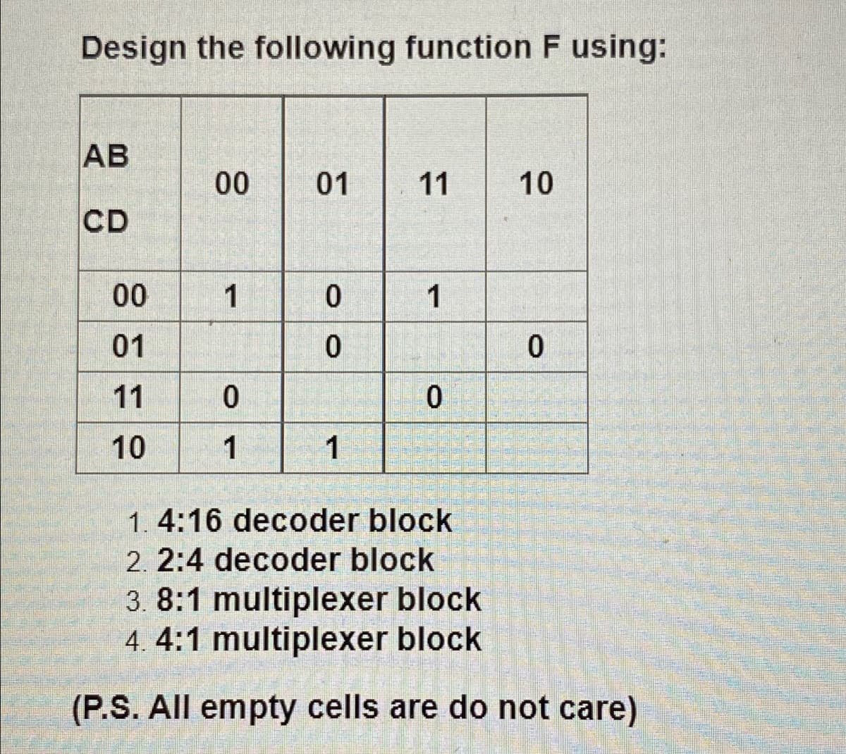
1. 4:16 decoder block 2. 2:4 decoder block 3. 8:1 multiplexer block 4. 4:1 multiplexer block


Q: What is the bit mask design to invert the bits in the position 0 through 3 of the register AL, while…
A: 1) We need to design a bitmask to invert the bits in position 0-3 of register AL 2) We have AND and…
Q: multiplexer is a device that connects __________________________. a. Single input line to a…
A: Multiplexing means combining various different types of input to one output, and the device used for…
Q: Write VHDL code for a Laser Circuit FSM that shows separate “blocks” for the next state decoder,…
A: In this work, a directional counter circuit is designed using light source and light sensor, up-down…
Q: Output Flag - 1 bit Interrupt Enable - 1 bit v each register is used.
A: Step by step with explanation is given below:
Q: 1. Design a 32-bit counter that will either increment by 4 or load a new 32-bit value, D, on each…
A: GIVEN:
Q: 4 x 4 decoder possible?
A: Decoder : Decoder is a combinational circuit that has ‘n’ input lines and maximum of 2n output…
Q: Write synthesizable VHDL code for a 5-to-10 decoder with an enable signal, active low, and outputs…
A: kindly check step 2 for code
Q: 1- Perform a comparison of the combinational circuit and the sequential circuit that realize the add…
A: Answer is given below-
Q: Two types of SPLDs are(a) CPLD and PAL (b) PAL and FPGA(c) PAL and GAL (d) GAL and SRAM
A: Two major types of simple programmable logic devices (SPLDs) are the PAL and GAL. PAL stands for…
Q: If the input frequency applied to given system is 640 KHz then the output frequency will be. kHz.…
A: Introduction :
Q: Describe the Lamport’s clock as opposed to physical clock
A: Given: Describe the Lamport’s clock as opposed to physical clock
Q: Fill in the table below by making the necessary explanation for each MUX signal (s2, s1, s0)…
A: In this section, let us execute 1x8 De-Multiplexer using 1x4 De-Multiplexers and 1x2 De-Multiplexer.…
Q: Explain Add Drop Multiplexers (ADM) and Terminal multiplexers (TM) and discuss where it can be used.
A: - The question wants to know about the add drop multiplexers and terminal multiplexers and their…
Q: (5) A 50usec square wave is applied to the INT1 input of an 8051 microcontroller. (a) Write the main…
A: Given:
Q: The sound output has data-rate of approximately a. 4 b. 6 c. 7 d. 8
A: Here, Four options are given.
Q: write assembly code for C=A-B for this accumulator architecture machine
A: The below program in assembly code
Q: (True/False): In video mode 13h, each screen row uses 320 bytes of storage.
A: The INT 10h can be used to draw graphics on the screen but it draws a single pixel on the screen at…
Q: 7) For an 8-to-1 multiplexer, a ________________ selection code is needed. a) 3 bit b) 2 bit c) 8…
A: Answer :-- a) 3 bit
Q: Specify the bits in the Single Mask register to clear bits in channel 0
A: A3 A2 A1 A0 IORN IOWN 1 0 1 0 1 0 X X X X D3 D2 D1 D0
Q: Describe the Lamport's clock in contrast to the physical clock.
A: Introduction: In each operation, a Lamport logical clock is a numerical software counter value.
Q: Build the 7 Segment Decoder and convert it into symbol (block).
A: Theory: A Digital Decoder IC, is a device that converts one digital format into another and one of…
Q: List the pins on Arduino that can do analog write.
A: Answer:- Arduino Uno is considered for calculating duty cycle and voltage values.
Q: How is multiplexer implemented in computer memory.
A: Introduction : We must examine how a multiplexer is implemented in computer architecture.
Q: Seven segment LED display (common cathode) is connected to port 2 of 8051 as shown in figure below.…
A: ANSWER: Seven Segment Display: A seven-segment display is a combination of eight LEDs connected in…
Q: Design a logism circuit that converts a 4-bit binary into base-9? Show screenshot of the circuit.
A: Answer has been explained below:-
Q: Line decoder is similar to demultiplexer except that there is _____ input line. a) two b) one c)…
A: De-multiplexer Decoder Takes one input line signals and produce multiple output lines It takes n…
Q: 8051 Assembling program: design a program Count down from 9000 to 8000, show it on 7-segment LED,…
A: SUMMARY: -Hence, We discussed all the points.
Q: Bit 11 of the D accumulator is also bit ___ of the ___ accumulator
A: 9) Bit 11 of the D accumulator is also bit ___ of the ___ accumulator
Q: ogram using Timer 0 to create a 10 kHz square wa
A: Below the Assembly Program using Timer 0 to create a 10 kHz square wave on P1.0?
Q: Bit Ripple Counter
A: clock output Q1 output Q2 output Q3 output Q4 output Q'1 output Q'2 output Q'3…
Q: Input Output -0.25 Input Output Input Output -4 4 0.125 -4 -64 -3 -0.33333 -3 0.25 -3 -27 -2 -0.5 -2…
A: NOTE: We are authorized to answer only the first three questions at a time when multi-part questions…
Q: Design 4 bit Flash ADC, with Vref = 12 v and Vin = 7.5 v.
A: Given data is shown below: Design 4 bit Flash ADC, with Vref = 12 v and Vin = 7.5 v.
Q: genel a squa wave KHZ mer 2 of the K-25 microcontroller
A: The 8051 has two timers: Timer 0 and Timer 1. They can be used either as timers or as event…
Q: Explain system calculator using full adder, multiplexer and decoder and design on proteus
A: A system calculator is an online tool which helps to find values. Manu computational algorithms…
Q: 3. For the multiplexer shown in the figure, write the truth table and draw the output waveform. 4x1…
A: In this question, we have to draw the output waveform and also write the truth table. In given 4x1…
Q: _is a device which takes single input and select one of many outputs to be connected to the single…
A: a. Seven segments display It is basically a 3x8 decoder that takes 3 input, but in the question…
Q: The number of local sequential devices (flops, latches) would need to increase from a nonpipelined…
A: In a non pipelined machine activities done like fetch the data, decode the data, and execute…
Q: Q1- Design and implement an Heart Pulse and Temperature Monitoring system using an 8051 as shown in…
A: heart rate monitor using 8051 microcontroller. The device senses the heart rate from the finger tip…
Q: Q6. Construct a code to generate a square wave of 100 Hz frequency on pin PORTB.2. Use timer 0, 16…
A: Solution:-- 1)The given question has required for the solution to be provided with the help of the…
Q: The basic storage element in a digital system is Select one: O a. multiplexer O b flipflop C.…
A: The basic storage element in digital system is
Q: 5: Design a 3x8 decoder using 1x2 decoder?
A: Actually, the answer has given below:
Q: Part A: Refer to figure 1, complete the output slots by using Synchronous and Statistical TDM. Line…
A: SYNCHRONOUS TDM the data flow of each input connection is divided into simple units and each units…
Q: Develop a series of functions for a 200 ms time delay called D200 if the microcontroller clock is 12…
A: SUMMARY: -Hence, We discussed all the points.
Q: esign 1 b
A: Step 1: ALU is a one-bit operation.The digital function that performs micro-operations on data…
Q: Example 1: 2 3 4 5 5 4 3 2 1 Input: head = [1,2,3,4,5] Output: [5,4,3,2,1]
A: First, we will add elements to the linked list. Then we will reverse the list using recursion. And…
Q: Write in detail about at least three the variants each of Branch and Shift instructions in a SRC
A: Branch Instructions Like many programming languages, HSAIL supports branch instructions that can…
Q: 2.2. Define Serial Communication, and name the 3 methods used by the Microcontroller: (No…
A: The answer is given below...
Q: F (A, B, C, D) = A'B + C'D + AD . What is the type of the decoder? (Example. 3-8 active high…
A: Decoder is a combinational logic circuit that converts coded input to coded outputs provided both of…
Q: The 74LS47 I.C. shown in the attached diagram is a: The circuit shown has a '1' on the data select…
A: According to the information given:- We have to choose the correct option to satisfy the statement.…
Q: The basic storage element in a digital system is ............. Select one: O a. multiplexer O b.…
A: The data I stored in memory .and flip flop is used to store a data because it is a memory.…

Step by step
Solved in 3 steps with 4 images


- A(n) _____ operation transforms a 0 bit value to 1 and a 1 bit value to 0.LIST P = 16F877AUsing INCLUDE "P16F877A.INC" and PWM (Pulse Width Modulation), write the microprocessor code that enables the fan to operate at 80% if the button on the 5th bit is pressed, and 30% if the button on the third bit is pressed.Consider this 1-bit ALU design, as shown in class (note that the rounded rectangles controlled by Ainvert, Binvert, and Operation represent multiplexers): If I want Result to be the result of a - b, then what value do each of these other inputs need to be? Ainvert : 0 or 1 Binvert : 1 or 0 CarryIn: 1 or 0 Operation : 00 , 01, 10, 11 which one ?
- Given a bit array A = [ 0 0 1 1 0 1] on which the operations are workable:i) Can you use OR to change any desired bit of A to 1?ii) Can you use AND to change any desired bit of A to 0?iii) Can you use XOR to invert or toggle any desired bit of A?In this exercise you are to construct an ALU with the following specification: • The ALU takes 3 different 32-bit inputs: A, B, C; and has one 32-bit output: D. • The ALU supports 7 different operations: – A + B (addition) – A - B (subtraction) – MAX(A,B,C) – MIN(A,B,C) – A & B (bitwise AND) – B & C (bitwise AND) – (A + B) & C (addition followed by bitwise AND) To construct this ALU you will follow a modular design. Assume you have an unlimited number of the following gates and combinational circuits at your disposal, but no others: • 2-arity AND gate, • 2-arity OR gate, • NOT gate, • 2-way MUX, • bit-wise AND circuit: it takes two 32-bit inputs and has a 32-bit output which is the bit-wise AND of its inputs. • 32-bit ADDER: it takes two 32-bit inputs, a 1-bit control signal, and has a 32-bit output. If the control signal is 0, the circuit outs the sum of its inputs. If the control signal is 1, the circuit outputs the difference of its inputs. The inputs and outputs are…Write a program that acquires data from a data source and calculates and displays the Discrete FourierTransform associated with that data. In this case, the Arduino will generate a signal, that is sampled by the ADC and then sent to the computerover the serial port. The Arduino code is : int lookup_index = 0; #define SIN_FREQ 100 long sin_freq = SIN_FREQ; #define LOOKUP_ARRAY_SIZE 128UL #define PWM_RESOLUTION 8 #if PWM_RESOLUTION <= 8 #define PWM_t uint8_t #else #define PWM_t uint16_t #endif PWM_t *lookup_array; // lookup array for sin(2pi f t) PWM_t lookup_array1[LOOKUP_ARRAY_SIZE] = { 127, 133, 139, 146, 152, 158, 164, 170, 176, 181, 187, 192, 198, 203, 208, 212, 217, 221, 225, 229, 233, 236, 239, 242, 244, 247, 249, 250, 252, 253, 253, 254, 254, 254, 253, 253, 252, 250, 249, 247, 244, 242, 239, 236, 233, 229, 225, 221, 217, 212, 208, 203, 198, 192, 187, 181, 176, 170, 164, 158, 152, 146, 139, 133, 127, 121, 115, 108, 102, 96, 90, 84, 78, 73, 67, 62,…
- Parity is a function in which the output depends on the number of 1s in the input. For an even parity function, the output is 1 if the input has an even number of ones. Suppose a ROM is used to implement an even parity function with a 4-bit input. Which of A, B, C, or D represents the contents of the ROM?Assume SP is 256, LOCAL is 300, ARGUMENT is 400, THIS is 3000, and THAT is 3010. Translate the following VM code into ASM code: push constant 7 push constant 3 add1. Evaluate the postfix 3 4 2 * + 9 - 2. Convert infix 5 * (6 + 7) to postfix
- 5.8 Write the function described in section 5.8 and a main routine to test it IN MIPS CREATE A CODE THAT READS DECIMAL VALUES AND DETECT ERRORDesign a sequence detector of the pattern 0100 where the circuit accepts a serial bit stream *X" as input and produces a serial bit stream *2° as outputWhenever the bit pattern *0100* appears in the input stream, it outputs 2 = 1: at all other times, 2 = Q Overlapping occurrences of the pattern are also detected,please answer asap DES: for the 16th round in DES, assume the output of 15th round is LE = 30A6, RE = DE7F, given the function F(RE, K_16) = A2F1. XOR operation is performed bit by bit. please calculate the entire output of 16th round in HEX representation