Draw the schematic circuit for a resistively loaded NMOS inverter and the relative voltage transfer characteristic where the different regions of operation of the transistor are shown.
Draw the schematic circuit for a resistively loaded NMOS inverter and the relative voltage transfer characteristic where the different regions of operation of the transistor are shown.

Introductory Circuit Analysis (13th Edition)
13th Edition
ISBN:9780133923605
Author:Robert L. Boylestad
Publisher:Robert L. Boylestad
Chapter1: Introduction
Section: Chapter Questions
Problem 1P: Visit your local library (at school or home) and describe the extent to which it provides literature...

Related questions
Question
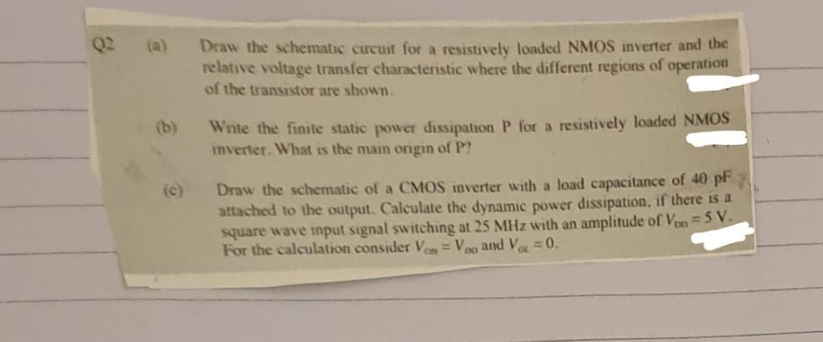
Transcribed Image Text:Q2
Draw the schematic circuit for a resistively loaded NMOS inverter and the
relative voltage transfer characteristic where the different regions of operation
of the transistor are shown.
(a)
Write the finite static power dissipation P for a resistively loaded NMOS
mverter. What is the main orgin of P?
(b)
Draw the schematic of a CMOS inverter with a load capacitance of 40 pF
attached to the output. Calculate the dynamic power dissipation, if there is a
square wave input signal switching at 25 MHz with an amplitude of Vpo=5 V.
For the calculation consider Vo= Vpo and V = 0.
(c)
%3D
DD
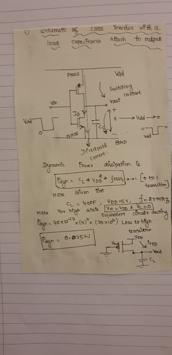
Transcribed Image Text:chematic
mvertes of th a
cntos
load
capeeftance
a Hach
to outpat
Pmos
Suitching
Vout
Vead
→Vdd o
Nmas
Vold
GND
Diret path
yramie
Curent-
Powes
důsipatfon &
Paun = * VDD*
[o to !
transition
Here
Giren that
CL = 40PF
Hor. high state
40 xto12
VDp =5Y, J=85MAZ
VH = VDD 2 Ve =0
Equialent
Here
Pagn=
x(5)x (25x105) LOw to high
transition
O.025W
VOD
CL
Expert Solution
This question has been solved!
Explore an expertly crafted, step-by-step solution for a thorough understanding of key concepts.

Step by step
Solved in 2 steps with 2 images

Knowledge Booster


Learn more about
Need a deep-dive on the concept behind this application? Look no further. Learn more about this topic, electrical-engineering and related others by exploring similar questions and additional content below.Recommended textbooks for you
Introductory Circuit Analysis (13th Edition)
Electrical Engineering
ISBN:
9780133923605
Author:
Robert L. Boylestad
Publisher:
PEARSON

Delmar's Standard Textbook Of Electricity
Electrical Engineering
ISBN:
9781337900348
Author:
Stephen L. Herman
Publisher:
Cengage Learning

Programmable Logic Controllers
Electrical Engineering
ISBN:
9780073373843
Author:
Frank D. Petruzella
Publisher:
McGraw-Hill Education
Introductory Circuit Analysis (13th Edition)
Electrical Engineering
ISBN:
9780133923605
Author:
Robert L. Boylestad
Publisher:
PEARSON
Delmar's Standard Textbook Of Electricity
Electrical Engineering
ISBN:
9781337900348
Author:
Stephen L. Herman
Publisher:
Cengage Learning
Programmable Logic Controllers
Electrical Engineering
ISBN:
9780073373843
Author:
Frank D. Petruzella
Publisher:
McGraw-Hill Education

Fundamentals of Electric Circuits
Electrical Engineering
ISBN:
9780078028229
Author:
Charles K Alexander, Matthew Sadiku
Publisher:
McGraw-Hill Education

Electric Circuits. (11th Edition)
Electrical Engineering
ISBN:
9780134746968
Author:
James W. Nilsson, Susan Riedel
Publisher:
PEARSON

Engineering Electromagnetics
Electrical Engineering
ISBN:
9780078028151
Author:
Hayt, William H. (william Hart), Jr, BUCK, John A.
Publisher:
Mcgraw-hill Education,