ECE 520 - VLSI Design (spring 2024) 1. Due in class: Thursday April 11, 2024 Homework #8 The following is the layout of an inverter with dimensions. Assume that VDD=2.5V, K'n=100uA/V², Vtn=0.4V, K'p=60uA/V², Vtp=-0.5V, tox=12nm, εox=3.9, Xd=42nm (overlap distance under the gate), C=0.74fF/um², Cjsw=0.43fF/um for both NMOS and PMOS devices at zero bias. a. Estimate the effective input capacitance of the inverter, Cin. b. Estimate the effective output capacitance of the inverter, Cout. For simplicity find effective Cout at zero bias. c. If the output of this inverter is connected to a similar inverter, estimate the tpHL and tpLH. Ignore the wire parasitic capacitance. GND A (input) 0.6um 0.6um Z (output) 0.5um ←>> 0.25um VDD 0.5um 0.25um
ECE 520 - VLSI Design (spring 2024) 1. Due in class: Thursday April 11, 2024 Homework #8 The following is the layout of an inverter with dimensions. Assume that VDD=2.5V, K'n=100uA/V², Vtn=0.4V, K'p=60uA/V², Vtp=-0.5V, tox=12nm, εox=3.9, Xd=42nm (overlap distance under the gate), C=0.74fF/um², Cjsw=0.43fF/um for both NMOS and PMOS devices at zero bias. a. Estimate the effective input capacitance of the inverter, Cin. b. Estimate the effective output capacitance of the inverter, Cout. For simplicity find effective Cout at zero bias. c. If the output of this inverter is connected to a similar inverter, estimate the tpHL and tpLH. Ignore the wire parasitic capacitance. GND A (input) 0.6um 0.6um Z (output) 0.5um ←>> 0.25um VDD 0.5um 0.25um

Introductory Circuit Analysis (13th Edition)
13th Edition
ISBN:9780133923605
Author:Robert L. Boylestad
Publisher:Robert L. Boylestad
Chapter1: Introduction
Section: Chapter Questions
Problem 1P: Visit your local library (at school or home) and describe the extent to which it provides literature...

Related questions
Question
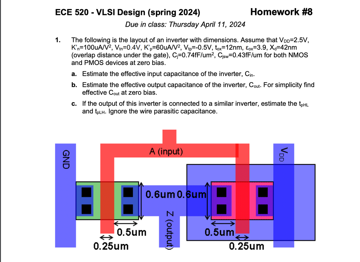
Transcribed Image Text:ECE 520 - VLSI Design (spring 2024)
1.
Due in class: Thursday April 11, 2024
Homework #8
The following is the layout of an inverter with dimensions. Assume that VDD=2.5V,
K'n=100uA/V², Vtn=0.4V, K'p=60uA/V², Vtp=-0.5V, tox=12nm, εox=3.9, Xd=42nm
(overlap distance under the gate), C=0.74fF/um², Cjsw=0.43fF/um for both NMOS
and PMOS devices at zero bias.
a. Estimate the effective input capacitance of the inverter, Cin.
b. Estimate the effective output capacitance of the inverter, Cout. For simplicity find
effective Cout at zero bias.
c. If the output of this inverter is connected to a similar inverter, estimate the tpHL
and tpLH. Ignore the wire parasitic capacitance.
GND
A (input)
0.6um 0.6um
Z (output)
0.5um
←>>
0.25um
VDD
0.5um
0.25um
Expert Solution
This question has been solved!
Explore an expertly crafted, step-by-step solution for a thorough understanding of key concepts.

This is a popular solution!

Trending now
This is a popular solution!

Step by step
Solved in 2 steps with 2 images

Recommended textbooks for you
Introductory Circuit Analysis (13th Edition)
Electrical Engineering
ISBN:
9780133923605
Author:
Robert L. Boylestad
Publisher:
PEARSON

Delmar's Standard Textbook Of Electricity
Electrical Engineering
ISBN:
9781337900348
Author:
Stephen L. Herman
Publisher:
Cengage Learning

Programmable Logic Controllers
Electrical Engineering
ISBN:
9780073373843
Author:
Frank D. Petruzella
Publisher:
McGraw-Hill Education
Introductory Circuit Analysis (13th Edition)
Electrical Engineering
ISBN:
9780133923605
Author:
Robert L. Boylestad
Publisher:
PEARSON
Delmar's Standard Textbook Of Electricity
Electrical Engineering
ISBN:
9781337900348
Author:
Stephen L. Herman
Publisher:
Cengage Learning
Programmable Logic Controllers
Electrical Engineering
ISBN:
9780073373843
Author:
Frank D. Petruzella
Publisher:
McGraw-Hill Education

Fundamentals of Electric Circuits
Electrical Engineering
ISBN:
9780078028229
Author:
Charles K Alexander, Matthew Sadiku
Publisher:
McGraw-Hill Education

Electric Circuits. (11th Edition)
Electrical Engineering
ISBN:
9780134746968
Author:
James W. Nilsson, Susan Riedel
Publisher:
PEARSON

Engineering Electromagnetics
Electrical Engineering
ISBN:
9780078028151
Author:
Hayt, William H. (william Hart), Jr, BUCK, John A.
Publisher:
Mcgraw-hill Education,