For the circuit shown below find (I,, I2, I;) and (Va, Vb, Ve, V.)

Delmar's Standard Textbook Of Electricity
7th Edition
ISBN:9781337900348
Author:Stephen L. Herman
Publisher:Stephen L. Herman
Chapter33: Single-phase Motors
Section: Chapter Questions
Problem 1PA

Related questions

Question
Delta - Star conversion
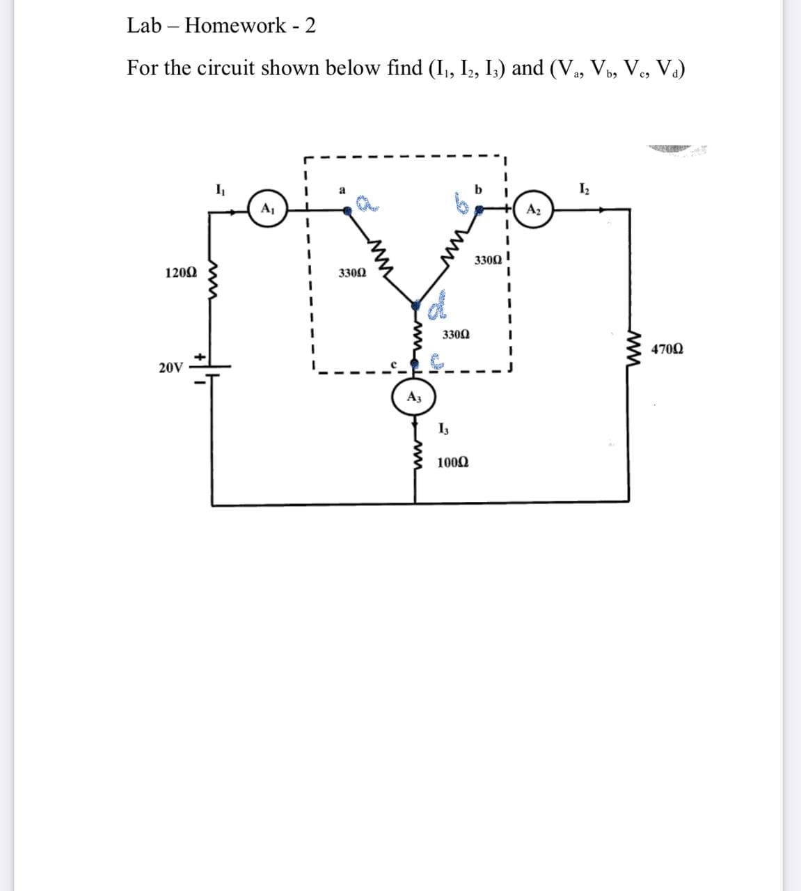
Transcribed Image Text:Lab – Homework - 2
For the circuit shown below find (I,, I2, I.) and (V, V, Ve, V.)
I
Iz
A,
A2
1200
3300 !
3300
3300
4700
20V
A3
I3
100Q
ww
Expert Solution
This question has been solved!
Explore an expertly crafted, step-by-step solution for a thorough understanding of key concepts.

Step by step
Solved in 2 steps with 4 images

Knowledge Booster


Learn more about
Need a deep-dive on the concept behind this application? Look no further. Learn more about this topic, electrical-engineering and related others by exploring similar questions and additional content below.Recommended textbooks for you
Delmar's Standard Textbook Of Electricity
Electrical Engineering
ISBN:
9781337900348
Author:
Stephen L. Herman
Publisher:
Cengage Learning
Delmar's Standard Textbook Of Electricity
Electrical Engineering
ISBN:
9781337900348
Author:
Stephen L. Herman
Publisher:
Cengage Learning