m LAMBDA=0.005 Cbd

Q: ', (m/s) 3- 2 1 -t (s) 10 12 2 4 -1 -2 -3+
A: Given at t=0, x=0 And from graph
Q: A bowling ball moves down the lane from x=2.80 cm to x, = -5.00 cm during the time interval from f =...
A: Average velocity of an object is given by total displacement covered by the body over given time. So...
Q: 1. What is the difference between synchronous binary counter and asynchronous binary counter? 2. Wha...
A:
Q: 4. The Dym equation du is a nonlinear evolution equation which arises in the study of the motion of ...
A: Given,∂u∂t=u3∂3u∂x3u(x,t)=(ax+bt)c
Q: Point charge A is on the r-axis at r = -3.00 cm. At x = 1.00 cm on the x-axis its electric field is ...
A: Given, The magnitude of charge at B is twice of charge at A. That is, QB=2QA The electric field at C...
Q: Given force BC = 170 N, what is force AC? ((Answer in whole numbers only. without units. No periods....
A: Given that: BC=170 Nθ=60°α=30° To determine the value of AC.
Q: Two particles are fixed to an x axis: particle 1 of charge q1 = 2.93 × 10⁻⁸ C at x = 28.0 cm and par...
A:
Q: Calculate the percentage error made in Stirling's formula. When (i) n = I| (ii) n = 10.
A: According to Stirling's formula, logen!=nlogen-n
Q: For a solid in which the occupation of the energy states is given by the Fermi- Dirac distribution, ...
A: The Fermi dirac distribution is defined as fE=1eE-EfkT+1 Where fE is the probability that a particl...
Q: An electric car is designed to run on a bank of batteries with a total potential difference of 23 V ...
A:
Q: Two equal disks of external radius R and internal radius Ř / 2 are loaded with positive and uniform ...
A: Let the two small ring section in two disks having charge dQ and area of dA. ...
Q: A 0.2 kg ball is bounced off the floor from a vertical height of 1.5m. The ball rebounds upward with...
A: Given that,The mass of the ball : m = 0.2 (kg)The height : h = 1.5 (m)The energy : 0.6 (J)Here we ne...
Q: Calculate resolution and depth of field for the following. (a) A light microscope with a wavelength ...
A: The wavelength of light in light microscope is given as, λl=560 nm The angular aperture of light mic...
Q: (i) A sound has a frequency of 880 Hz, define what frequency means.
A: Given, The frequency of sound is 880Hz.
Q: 7. The resistivity of intrinsic Si is 2.3 x 10 . m at 300 K. Calculate its resistivity at 100°C. Ass...
A:
Q: What is the value of the magnitude of a vector if it is equal to the positive square root of the sum...
A: Answer : We know , the magnitude of a vector , A→ = Ax i^ + Ay j^ + Az k^ is : ...
Q: MT NUIES ASA TUUM IEACHER PRAC The helicopter view in the figure shows two people pulling on a stubb...
A: Force, F1=82.8 N , θ1=65.0°Force, F2=78.9 N, θ2=72.0° (making an angle with the negative x-axis)The ...
Q: A diatomic molecule has 18 x 10-5 eV of rotational energy in the I = 7 quantum %3D state. What is it...
A: Given, for j=7 rotational energy of diatomic moleculeEj=7=1.8×10⁻⁵ eVWe know that,Rotational energy ...
Q: Two point charges q4= 212.0 µCand qB= 45.0 µC and a third particle with unknown charge qcare located...
A:
Q: 2. Twin A makes a round trip at 0.6c to a star 12 light-years away, while twin B stays on the earth....
A: Given: v=0.6c, L0=12 light years, t=1year The time taken by twin A for twin B to cover the distance ...
Q: What is the wavelength of an electron moving at 3.00% of the speed of light?
A: By using de-broglie's theoryλ=hpwhere p=mv∴λ=hmv Equation 1given, v is 3% of c=3×3 x 108 m/s.10...
Q: In the X-ray analysis of a crystal element (cubic structure is unknown), the reflection angles are 4...
A: Given, reflection angles are400580730100.40114.70andλ=0.154 nm
Q: What double-slit separation would produce a first-order maximum at 3.00° for 25.0-keV x rays? The sm...
A: The equation for Constructive interference for a double-slit:- dsinθ = nλ Equation 1 where, d is t...
Q: The nuclear spin of the ground state of 140Pr according to the shell model:
A: Pr 140 has atomic number Z=59. The number of neutrons N = 81. The atomic mass A = 140 Both the numbe...
Q: The electric field vector in a region of space is given by the function of E=5xi +2yj where x and y ...
A: Given data, Electric field is : E→=5xi^+2y2j^ Points are : A(1,2) and B(3,5)
Q: Problem 4. A pot absorbs 84.6 kJ ±0.5 kJ of heat from the stove, and in the same time it loses 21.1 ...
A: Solution: 4. The heat absorbed by the pot is: Q1=84.6 kJ ±0.5 kJ The heat lost by the pot is: Q2=21....
Q: equattion : S/4 (1- a) = f*sigma*TS4 Solar Constant (W/m2) S = 1361 How sensitive is the temperat...
A: The solar constant is given as, S=1361 W/m2 The atmospheric transmittivity is given as, f=0.62 TO DE...
Q: Liquefied natural gas (LNG) in a vertical storage tank has a density of 455 kg/m³. The depth of LNG ...
A: The force exerted per unit area on a substance boundaries is referred to as pressure. Newton per Sq ...
Q: (i) A sound has a frequency of 880 Hz, define what frequency means. Define what is meant by periodic...
A: Simple Harmonic motion has several major characteristics, including frequency and periodic time. Thi...
Q: Below is a position graph of an object. What is the instantaneous velocity of the object at t= 3.5 s...
A:
Q: I HB: passes through inhomogeneous magnetic field, as in the Stern-Gerlach apparatus shown schematic...
A: Given: The field gradient is ∂B∂z=103 Tm-1. The distance between the pole and the screen i...
Q: The angular momentum of a flywheel having a rotational inertia of 0.983 kg-m2 about its central axis...
A: "Since you have posted a question with multiple sub-parts, we will solve first three sub parts for ...
Q: A flat circular loop of with radius R lies in the xy-plane centered at the origin. Its linear charge...
A:
Q: aut a 12-V a.8) Design an astable circuit that gives p-p (ov to 12v) output pulae waveform whos e pu...
A:
Q: a b d f N h W E S 10 20 30 40 km Answer Bank 30 km, 78° south of east 10 km, northwest 25 km, east b...
A: The tail of the vector is the point of starting if the tail of the vector taking as the origin and t...
Q: A student used a video camera to record another student dropping a marble through water in a graduat...
A: The marble is dropped in the graduated cylinder which consists of water in it. The marble is droppe...
Q: 79. A hockey player hits a "slap shot" in practice at a horizontal distance of 15 m from the nết (wi...
A: Given velocity of puck, At 5.0° above horizontalV0=50 m/secHorizontal component of Initial velocity,...
Q: Given force AC = 400 N, what is force BC? ((Answer in whole numbers only, without units. No periods....
A: Given that: AC=400 Nto determine the value of BC
Q: 5Ocm hde is cut ina large piece of cardboard A paind saurce is placed 3.0 m directy behind the hole,...
A: The radius of the hole is 2.5cm. (a) The rays diverge from the source, pass through the hole, and f...
Q: The 4 nF capacitors are pre-charged to 3 V, and the 10 nF capacitor is pre-charged to 1.2 V. At t = ...
A: Let C1 = 4 nF C2 = 4 nF C3 = 10 nF Initially, V1 = 3 V V2 = 3 V V3 = 1.2 V
Q: 33. In a parallel projection, will a line parallel to the Z axis project as a point, a line, or not ...
A: A line parallel to the z-axis has certain fixed values of x and y and a variable value of z. If a ...
Q: P3- A particle of mass 0.32 kg is attached to the end of an inextensible cord of length 0.96 m. Wher...
A: (Only the 15th part of the question has been asked to solve) mass of the particle, m=0.32 Kg Length ...
Q: create an acceleration time graph and velocity time graph based on the attached image.
A:
Q: The principle of the AGC circuit in AM receiver by the amplifier gain increases when the DC feedback...
A: To answer: The principle of the AGC circuit in the AM receiver:
Q: A proton is placed in a uniform electric field of 3000 N/C. You may want to review (Page). Part A Fo...
A:
Q: An infinitely long line charge with uniform positive charge density A1 lies on the y axis as shown i...
A: option a is the correct answer.
Q: In a vertical gate of a small dam there is a window at a distance a per below the surface of the liq...
A: Hydrostatic force is given by: F=PA Here, P is pressure and A is area. Also pressure is defined as P...
Q: A proton accelerates from rest in a uniform electric field of 650 N/c. At one later moment, its spee...
A: Given : E=650N/C, v=1.2×10⁶m/s The acceleration of the proton due to the electric field is found b...
Q: 3. It is September of 1936, and the Kenyan aviatrix Beryl Markham is attempting the first solo fligh...
A:
Q: nd Fg 40.0N. where N is the standard Sl unit of force. What is F3 in unit-vector notation?
A:
Simulate in LTSPICE Please, model file is as under:
.model nch_lev2 NMOS (LEVEL=2 VTo=1.4 Kp=.6m LAMBDA=0.005 Cbd=100f Cbs=100f)
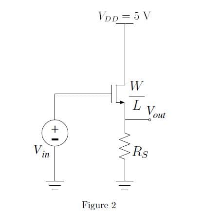
![] We wish to design the CMOS common-drain amplifier shown in Fig. 2 so that Ip = 200 µA,
Im = 2 ms, and the de output voltage is 2.0V. Setting the transistor length to 2µm and using
the given model parameters find the values of Rs, the transistor width, and the de input
voltage.
] Run the dc operating point analysis and verify that the design parameters specfieid in [Sim
4.] are realized. Note the small-signal parameters and device capacitances Cgs, Cgd, Cbs, and
Cbd and then estimate the dominant pole of the amplifier.](/v2/_next/image?url=https%3A%2F%2Fcontent.bartleby.com%2Fqna-images%2Fquestion%2Fda60d662-3926-4137-a01a-496e36dbee5c%2Fbd0dd2a2-866b-448e-a88f-fed9fa6e4854%2Fh6jrrcs_processed.jpeg&w=3840&q=75)


Trending now
This is a popular solution!

Step by step
Solved in 2 steps with 4 images
