Now we can determine the value for the W/L ratio of the NMOS switching device from the MOS drain current expression using the circuit conditions in Fig. 6.12(b). In this case, the input is set equal to V = 2.5 V, and the output of the inverter should then be at V. The expression for the drain current in the triode region of the device is used because vGS - VTN = 2.5 V-0.6 V = 1.9 V, and vps = V = 0.20 V, yielding vps < vGs – VyN- VDD = 2.5 V IpD 28.8 k2 o vo = VL 80 μΑ Ms + Vos = 0.20 V 2.22 Uj = Vµ=2.5 V EXERCISE: Redesign the logic gate in Fig. 6.12 to operate at a power of 0.4 mW while main- taining V = 0.20 V. %3D ANSWER: (W/L)s= 4.44/1; R= 14.4 k2
Now we can determine the value for the W/L ratio of the NMOS switching device from the MOS drain current expression using the circuit conditions in Fig. 6.12(b). In this case, the input is set equal to V = 2.5 V, and the output of the inverter should then be at V. The expression for the drain current in the triode region of the device is used because vGS - VTN = 2.5 V-0.6 V = 1.9 V, and vps = V = 0.20 V, yielding vps < vGs – VyN- VDD = 2.5 V IpD 28.8 k2 o vo = VL 80 μΑ Ms + Vos = 0.20 V 2.22 Uj = Vµ=2.5 V EXERCISE: Redesign the logic gate in Fig. 6.12 to operate at a power of 0.4 mW while main- taining V = 0.20 V. %3D ANSWER: (W/L)s= 4.44/1; R= 14.4 k2

Introductory Circuit Analysis (13th Edition)
13th Edition
ISBN:9780133923605
Author:Robert L. Boylestad
Publisher:Robert L. Boylestad
Chapter1: Introduction
Section: Chapter Questions
Problem 1P: Visit your local library (at school or home) and describe the extent to which it provides literature...

Related questions
Question
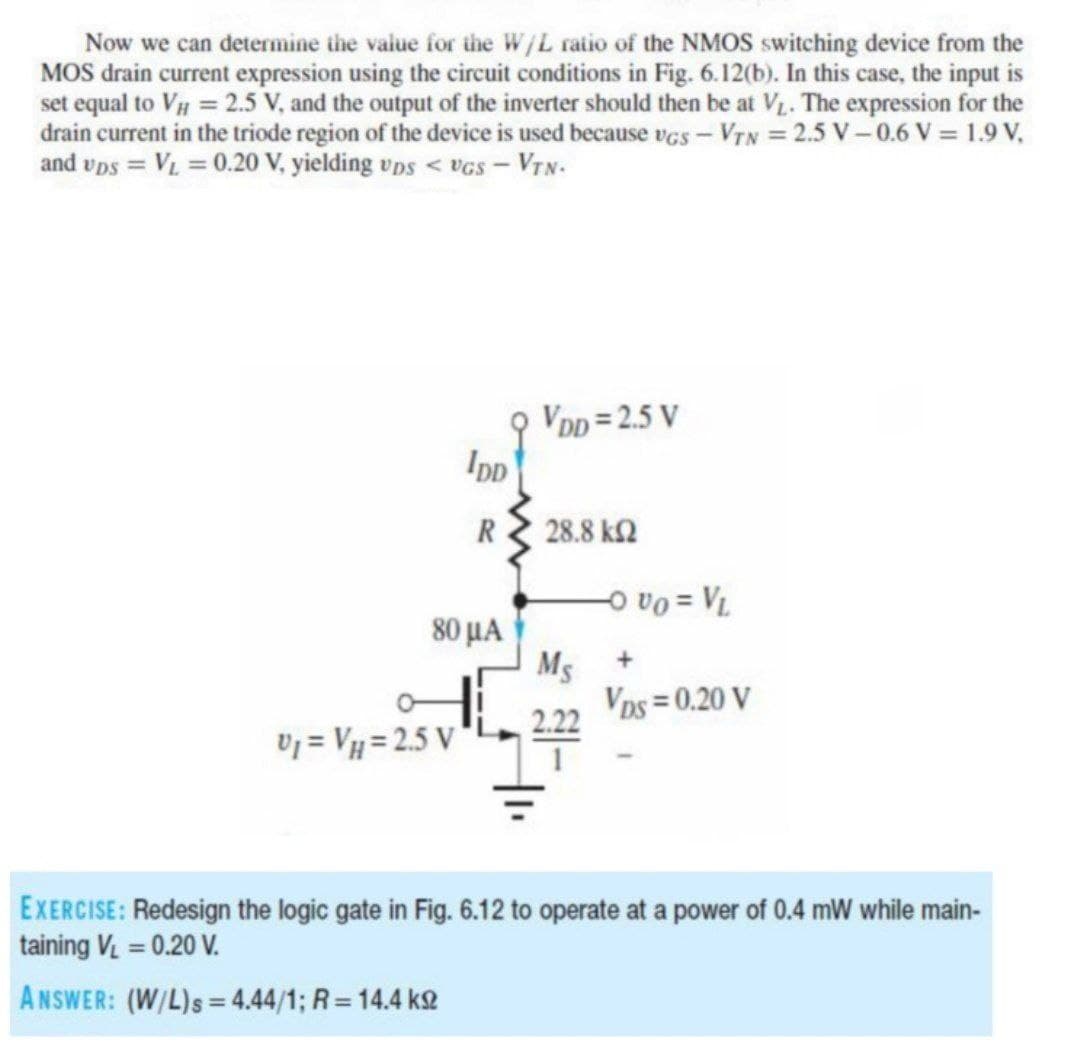
Transcribed Image Text:Now we can determine the value for the W/L ratio of the NMOS switching device from the
MOS drain current expression using the circuit conditions in Fig. 6.12(b). In this case, the input is
set equal to V = 2.5 V, and the output of the inverter should then be at V. The expression for the
drain current in the triode region of the device is used because vGS - VTN = 2.5 V-0.6 V = 1.9 V,
and vps = V = 0.20 V, yielding vps < vGs – VyN-
VDD = 2.5 V
IpD
R
28.8 k2
80 μΑ
A = 0a o
Ms +
Vos = 0.20 V
2.22
Uj = Vµ = 2.5 V
EXERCISE: Redesign the logic gate in Fig. 6.12 to operate at a power of 0.4 mW while main-
taining V = 0.20 V.
ANSWER: (W/L)s= 4.44/1; R= 14.4 k2
Expert Solution
This question has been solved!
Explore an expertly crafted, step-by-step solution for a thorough understanding of key concepts.

Step by step
Solved in 3 steps with 3 images

Knowledge Booster


Learn more about
Need a deep-dive on the concept behind this application? Look no further. Learn more about this topic, electrical-engineering and related others by exploring similar questions and additional content below.Recommended textbooks for you
Introductory Circuit Analysis (13th Edition)
Electrical Engineering
ISBN:
9780133923605
Author:
Robert L. Boylestad
Publisher:
PEARSON

Delmar's Standard Textbook Of Electricity
Electrical Engineering
ISBN:
9781337900348
Author:
Stephen L. Herman
Publisher:
Cengage Learning

Programmable Logic Controllers
Electrical Engineering
ISBN:
9780073373843
Author:
Frank D. Petruzella
Publisher:
McGraw-Hill Education
Introductory Circuit Analysis (13th Edition)
Electrical Engineering
ISBN:
9780133923605
Author:
Robert L. Boylestad
Publisher:
PEARSON
Delmar's Standard Textbook Of Electricity
Electrical Engineering
ISBN:
9781337900348
Author:
Stephen L. Herman
Publisher:
Cengage Learning
Programmable Logic Controllers
Electrical Engineering
ISBN:
9780073373843
Author:
Frank D. Petruzella
Publisher:
McGraw-Hill Education

Fundamentals of Electric Circuits
Electrical Engineering
ISBN:
9780078028229
Author:
Charles K Alexander, Matthew Sadiku
Publisher:
McGraw-Hill Education

Electric Circuits. (11th Edition)
Electrical Engineering
ISBN:
9780134746968
Author:
James W. Nilsson, Susan Riedel
Publisher:
PEARSON

Engineering Electromagnetics
Electrical Engineering
ISBN:
9780078028151
Author:
Hayt, William H. (william Hart), Jr, BUCK, John A.
Publisher:
Mcgraw-hill Education,