One way to manufacture transistors, which amplify electrical signals, is to diffuse impurity atoms into a semiconductor material such as silicon. Suppose a silicon wafer 0.1 cm thick, which originally contains 1 phosphorous (P) atoms for every 10 million Si atoms, is treated so that there are 400 P atoms for every 10 million Si atoms at the surface. Calculated the concentration gradient (a) in atomic percent/cm and (b) in atoms/cm3.cm. The lattice parameter of silicon is 5.4307 Å. Hint: Silicon is in a diamond cubic 400 P atoms Cs 107 Si atoms Structure with 8 atoms/cell. Silicon wafer Ax = 0.1 cm 1 P atom 107 Si atoms 55
One way to manufacture transistors, which amplify electrical signals, is to diffuse impurity atoms into a semiconductor material such as silicon. Suppose a silicon wafer 0.1 cm thick, which originally contains 1 phosphorous (P) atoms for every 10 million Si atoms, is treated so that there are 400 P atoms for every 10 million Si atoms at the surface. Calculated the concentration gradient (a) in atomic percent/cm and (b) in atoms/cm3.cm. The lattice parameter of silicon is 5.4307 Å. Hint: Silicon is in a diamond cubic 400 P atoms Cs 107 Si atoms Structure with 8 atoms/cell. Silicon wafer Ax = 0.1 cm 1 P atom 107 Si atoms 55
Introduction to Chemical Engineering Thermodynamics
8th Edition
ISBN:9781259696527
Author:J.M. Smith Termodinamica en ingenieria quimica, Hendrick C Van Ness, Michael Abbott, Mark Swihart
Publisher:J.M. Smith Termodinamica en ingenieria quimica, Hendrick C Van Ness, Michael Abbott, Mark Swihart
Chapter1: Introduction
Section: Chapter Questions
Problem 1.1P

Related questions
Question
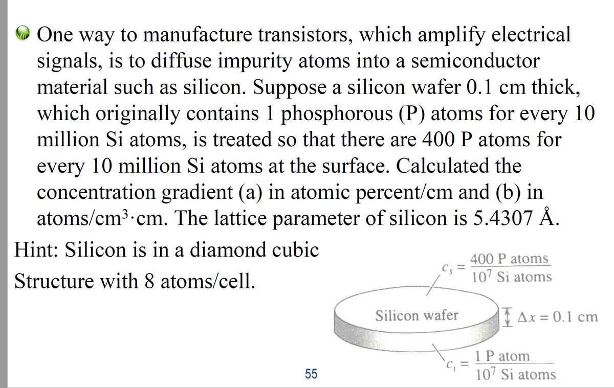
Transcribed Image Text:O One way to manufacture transistors, which amplify electrical
signals, is to diffuse impurity atoms into a semiconductor
material such as silicon. Suppose a silicon wafer 0.1 cm thick,
which originally contains 1 phosphorous (P) atoms for every 10
million Si atoms, is treated so that there are 400 P atoms for
every 10 million Si atoms at the surface. Calculated the
concentration gradient (a) in atomic percent/cm and (b) in
atoms/cm3.cm. The lattice parameter of silicon is 5.4307 Å.
Hint: Silicon is in a diamond cubic
400 P atoms
Cs =
107 Si atoms
Structure with 8 atoms/cell.
Silicon wafer
Δx -0.I cm
1 P atom
10 Si atoms
%3D
55
Expert Solution
This question has been solved!
Explore an expertly crafted, step-by-step solution for a thorough understanding of key concepts.

This is a popular solution!

Trending now
This is a popular solution!

Step by step
Solved in 2 steps with 2 images

Knowledge Booster


Learn more about
Need a deep-dive on the concept behind this application? Look no further. Learn more about this topic, chemical-engineering and related others by exploring similar questions and additional content below.Recommended textbooks for you
Introduction to Chemical Engineering Thermodynami…
Chemical Engineering
ISBN:
9781259696527
Author:
J.M. Smith Termodinamica en ingenieria quimica, Hendrick C Van Ness, Michael Abbott, Mark Swihart
Publisher:
McGraw-Hill Education
Elementary Principles of Chemical Processes, Bind…
Chemical Engineering
ISBN:
9781118431221
Author:
Richard M. Felder, Ronald W. Rousseau, Lisa G. Bullard
Publisher:
WILEY
Elements of Chemical Reaction Engineering (5th Ed…
Chemical Engineering
ISBN:
9780133887518
Author:
H. Scott Fogler
Publisher:
Prentice Hall
Industrial Plastics: Theory and Applications
Chemical Engineering
ISBN:
9781285061238
Author:
Lokensgard, Erik
Publisher:
Delmar Cengage Learning
Unit Operations of Chemical Engineering
Chemical Engineering
ISBN:
9780072848236
Author:
Warren McCabe, Julian C. Smith, Peter Harriott
Publisher:
McGraw-Hill Companies, The